鑫景福致力于滿足“快速服務(wù),零缺陷,輔助研發(fā)”PCBA訂購(gòu)單需求。


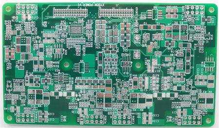
PCB制造

Influence of Weldability of Plate Holes on Welding Quality
Solderability means that the metal surface is wetted by molten solder, that is, a continuous, relatively uniform and smooth adhesive film is formed on the metal surface where the solder is located. Poor solderability of circuit board holes will cause faulty soldering defects and affect the parameters of components in the circuit. Unstable Multilayer board components and inner wires conduct, whICh will lead to the functional failure of the whole circuit in serious cases.

Solderability of circuit board is affected by the following PCB factors:
(1) Composition of welding materials and properties of materials to be welded. As an important part of the welding chEMIcal treatment process, the welding materials include the chemical materials with flux. Generally, the low melting point eutectic metal is Sn Pb or Sn Pb Ag, in which the impurity content cannot exceed a certain proportion to prevent impurities from producing oxides and being dissolved by the flux. The white rosin and isopropanol solvent are generally used as the welding flux to remove the corrosion on the surface of the circuit board through heat transfer, so as to help the solder better wet the surface of the circuit board to be welded.
(2) The solderability of the circuit board is also affected by the welding temperature and the cleanness of the metal plate surface. Too high temperature will accelerate the diffusion rate of solder, improve the activity of solder, cause rapid oxidation of PCB and solder melting surface, and form welding defects; Contaminated circuit board surface will also affect the solderability of the circuit board, resulting in solder beads, solder balls, open circuit, poor gloss and other defects.
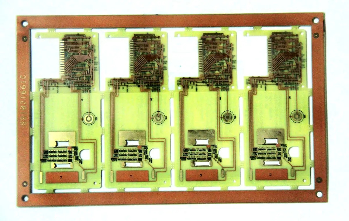
Welding defects caused by warping
During the welding process of PCB circuit boards and components, due to stress deformation and warping, there are defects such as faulty soldering and short circuit. The temperature imbalance between the upper and lower parts of the circuit board is the main cause of the circuit board warping. For large circuit boards, falling weight will also cause warping. The distance between an ordinary PBGA device and a circuit board is about 0.5mm. If the device on the circuit board is large, the circuit board will gradually return to its normal shape after cooling, and the stress will act on the solder joint for a long time. At this time, if the device is raised by 0.1mm, it is completely possible to cause a false solder open circuit.
Welding quality is affected by circuit board design
Although it is easy to control when welding on a PCB circuit board with large layout size, excessive board size will lead to long print lines, increased impedance, reduced noise resistance and increased board cost; When the size of the plate is too SMAll, the heat dissipation capacity decreases, the welding process is not easy to control, and adjacent lines interfere with each other. Therefore, the design of PCB must be optimized:
(1) Shorten the connection between high-frequency components as much as possible to reduce electromagnetic interference.
(2) The heavy components with a weight of more than 20g shall be fixed with brackets before welding.
(3) Heat dissipation shall be considered for heating elements to prevent defects caused by high surface temperature of elements. Thermal sensors shall be as far away from the heat source as possible.
(4) In order to make the circuit board beautiful and easy to weld, the components should be arranged in parallel as far as possible, which is also conducive to mass production. The optimal proportion of the circuit Board Design should be a 4 ∶ 3 rectangle. The wire width shall be balanced as far as possible to prevent discontinuous wiring. Large area copper foil should be avoided to prevent it from expanding and falling off when the circuit board is heated for a long time.


抖音二維碼

Q Q二維碼

微信二維碼
點(diǎn)擊
然后
聯(lián)系
然后
聯(lián)系
電話熱線
13410863085Q Q

微信

- 郵箱