鑫景福致力于滿足“快速服務(wù),零缺陷,輔助研發(fā)”PCBA訂購單需求。


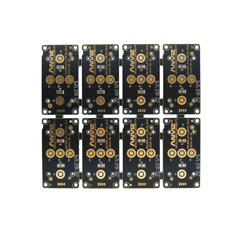
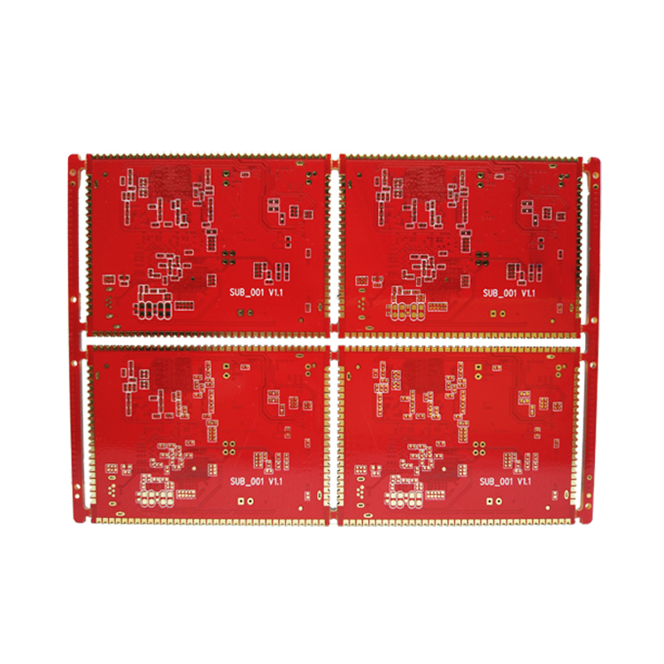
PCB制造
Calibration circuit and fault diagnosis in pcb circuit board function test
PCB manufacturers, PCB designers and PCBA manufacturers explain the calibration circuit and fault diagnosis in the functional test of PCB PCB
Calibration circuit
Function test is often used for calibration or verifICation of analog circuits, including checking the interior of UUT (such as the IF part of RF circuit) to verify its work. To do this, test points or test pads may be required. One problem in high frequency design is that the relative impedance of the test point (path length, test pad size, etc.) plus the impedance of the probe will affect the performance of the circuit. This should be kept in mind when setting the test area. Automatic mechanical detection and needle bed fixture (discussed later in this article) only need a SMAll test area to ease this contradiction, mainly because compared with manual operation, The accuracy of the robot itself allows the tester to detect smaller areas.
fault diagnosis
If only functional test is used as pass/fail filter without measuring calibration point, this section can be skipped, because the probe may not be used in this application. In most cases, the function test is passed/faiLED because the function test is very slow in diagnosing faults, especially in the case of multiple faults. However, in some industries, functional testing is going deep into the manufacturing process, such as the manufacturing of cellular phones. Some manufacturers need to conduct certain key measurements at the PCB level, that is, during the assembly process before final assembly, which is determined by the nature of mobile phones that are easy to be eliminated. In other words, mobile phones are designed to be assembled at a lower cost, and they are not easy to disassemble. Therefore, functional verification before final testing can save rework costs and reduce possible waste products (because mobile phones will be damaged when disassembled).
Therefore, sufficient test points are required to probe PCB. For example, it is not convenient to check the J-shaped lead of a surface mounted device with a spacing of 20 mil, and BGA is even less possible. According to the recommendations of SMTA, the minimum spacing between test points is 0.040 inch. The spacing between pads depends on the element height, probe size, etc. around the test area. However, 0.200 inch spacing should be the minimum requirement, especially for manual exploration areas. Obviously, test fixtures and robotic probes are more accurate.
PCB manufacturers, PCB designers and PCBA manufacturers will explain the calibration circuit and fault diagnosis in the functional test of pcb PCB.


抖音二維碼

Q Q二維碼

微信二維碼
點擊
然后
聯(lián)系
然后
聯(lián)系
電話熱線
13410863085Q Q

微信

- 郵箱