鑫景福致力于滿足“快速服務,零缺陷,輔助研發”PCBA訂購單需求。


PCB制造
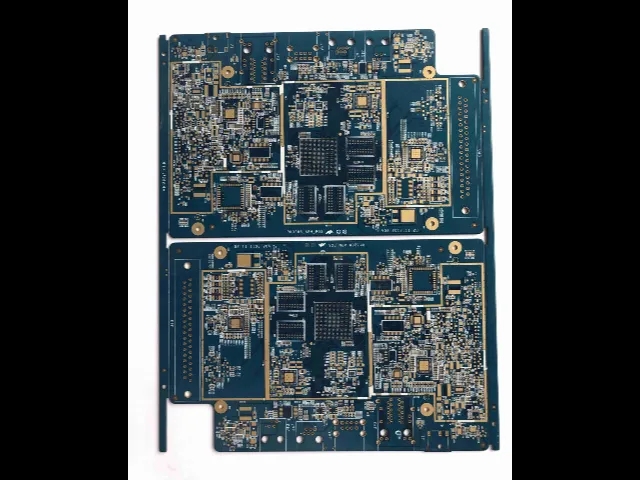
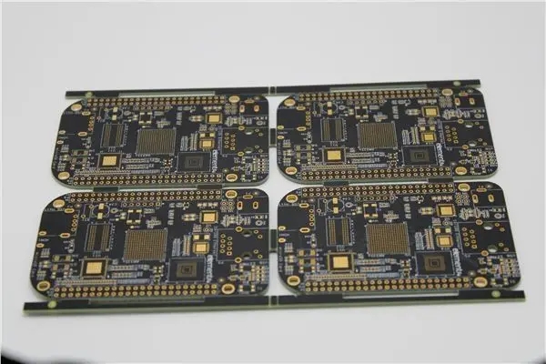
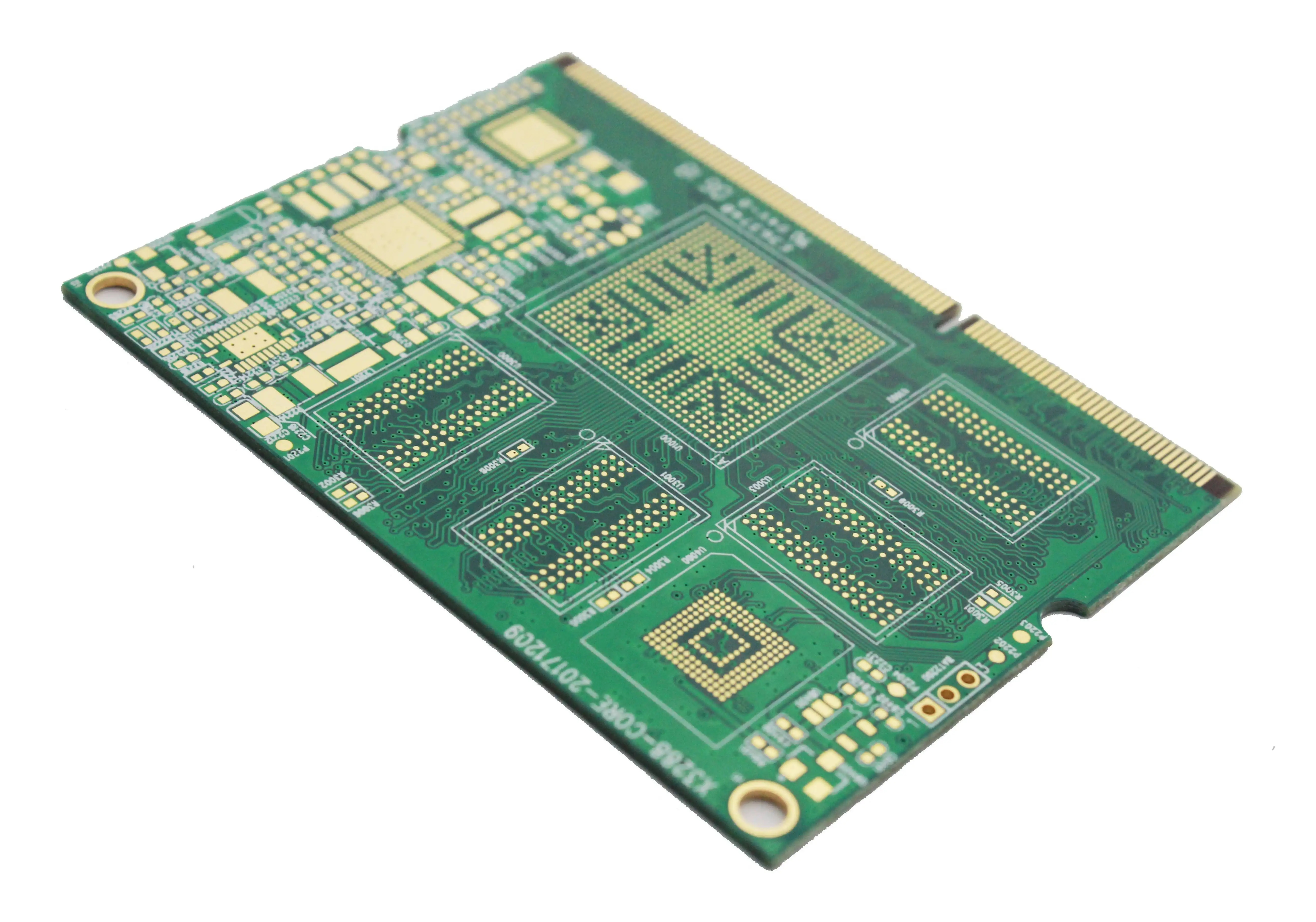
PCB solder resistance - detaiLED explanation of usage and process
There are three types of resistance welding commonly used for PCB: spot welding, seam welding and butt welding. However, problems often occur during the resistance welding process, including substrate bruise, false copper exposure, uneven resistance welding, and internal circuit fracture. In the production process, we will ensure that we pay attention to the key points of each step when dealing with resistance welding, and ensure to provide customers with high-quality PCB.
First of all, why do we do resistance welding. The purpose of resistance welding mainly includes the following points:
Leave the through-hole and its pad on the PCB to be soldered, cover all lines and copper surfaces, prevent short circuit caused by PCB wave soldering, and save the amount of soldering tin.
2. Prevent the damage of moisture and various electrolytes from oxidizing the circuit and damaging the electrICal performance, and prevent external mechanical damage to maintain good insulation of the board.
3. The thinner the boards are, the thinner the line width is, so the insulation problem between conductors is becoming increasingly prominent, which also increases the importance of the insulation performance of anti welding paint.
Secondly, people in the PCB industry know that solder mask refers to the part of the board surface that needs to be evenly coated with green paint. However, in fact, the green oil solder mask uses negative output, so after the shape of the green oil solder mask is mapped to the board, it is not green oil solder mask, but copper skin is exposed. In the production process, in order to increase the thickness of the copper sheet, the method of scribing on the solder mask will be used to remove the green oil. The solder mask plays an important role in controlling the welding defects in the reflow soldering process. The PCB designer should try to reduce the spacing or air gap around the pad during the design, or it can be handed over to our engineers.
For resistance welding process, Xiao Bian believes that there will be too many changes at present, but process innovation is everywhere, and the future development of PCB production and processing will encounter various challenges. Materials, equipment and PCB manufacturers will face challenges and even great pressure to survive. DoMEStic PCB manufacturers are at a relative disadvantage in such fields as HDI, automobile board and IC carrier board, and need more investment. Material suppliers, equipment suppliers and manufacturers are required to achieve closer cooperation beyond the SIMple interest relationship. Of course, different enterprises need to position their products differently. They should not all develop towards HDI, automotive electronic PCB boards, and IC packaging substrates. For enterprises, it is not the more difficult the better, nor the more sophisticated the better. What is suitable for them is the best.
PCB manufacturing, PCB design and PCBA processing manufacturers will explain PCB solder resistance - usage and process.


抖音二維碼

Q Q二維碼

微信二維碼
點擊
然后
聯系
然后
聯系
電話熱線
13410863085Q Q

微信

- 郵箱