鑫景福致力于滿(mǎn)足“快速服務(wù),零缺陷,輔助研發(fā)”P(pán)CBA訂購(gòu)單需求。


PCB制造
Processing technology, cost and surface treatment of PCB BGA components
Process and cost considerations of the processing manufacturer
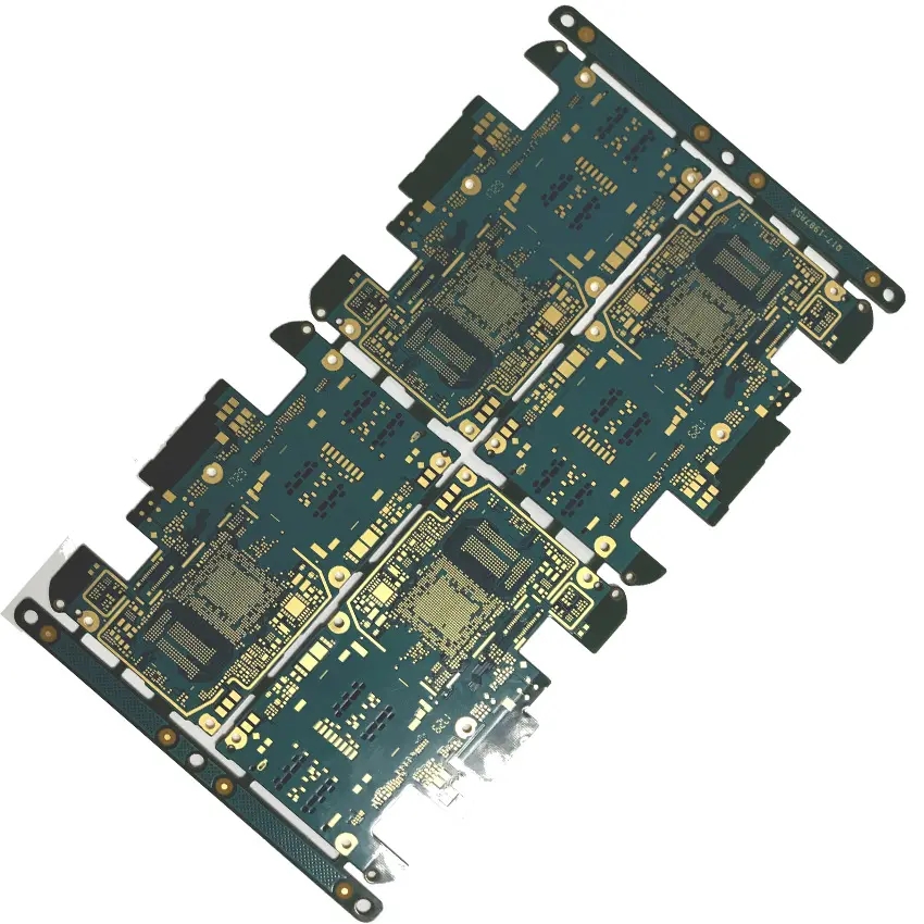
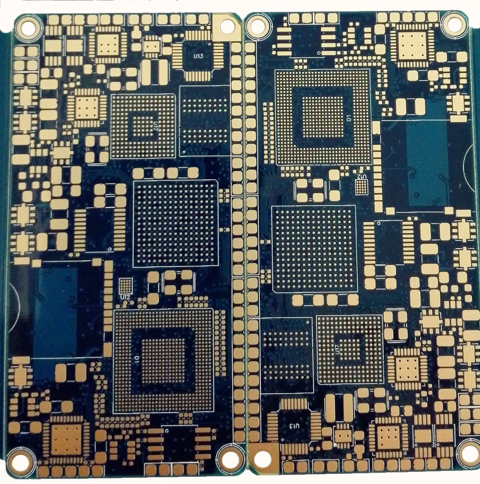
When designing a PCB containing BGA devices, in addition to the design on the technICal function level, it is also necessary to communicate with the corresponding PCB manufacturers with this processing capability. Including manufacturing process and corresponding cost. Different processing technologies will affect the mounting difficulty and the yield of products in the future.
In terms of processing technology, laser blind hole process requires VCP side spraying pulse electroplating copper to fill the blind hole, and after grinding, do negative acid etching to ensure the integrity of BGA. After etching, the final size of BGA is 0.27mm~0.28mm. In addition, due to the SMAll spacing of BGA, attentions shall be paid during processing;
1. Compensation treatment of BGA in engineering design to ensure the requirements of final bonding pad;
2. resistance welding and window opening to ensure that the window opening cannot be on the BGA pad, otherwise the mounting will be affected;
3. For the selection of printing ink, the green printing ink with high viscosity is preferred due to the small spacing;
4. Selection of surface treatment process. Generally, relatively flat surface treatment process is selected for BGA packaged PCB board surface treatment to ensure the best placement effect of the following chip solder ball and PCB board;
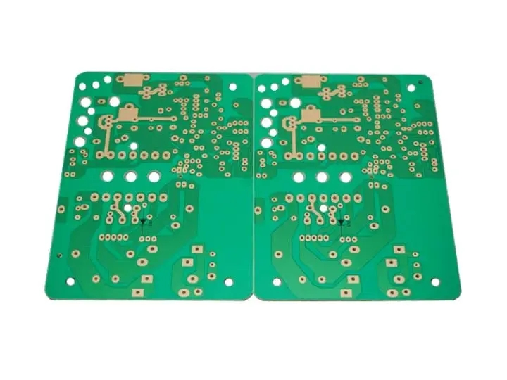
Surface technology includes: hot air leveling, gold deposition, silver melting, tin melting, OSP and other surface technologies. OSP has the best solderability, but attention should be paid to protect the oxide film from oxidation and scratch. The example PCB used in this paper can be used for OSP surface processing. PCB surface shall be mounted within 3 months after OSP, otherwise welding will be affected. The cost of OSP surface treatment process is relatively low.
Now let's popularize the surface treatment process of PCB processing and manufacturing:
Purpose of PCB surface treatment:
The basic purpose of surface treatment is to ensure good weldability or electrical performance. As the copper in nature tends to exist in the form of oxide in the air, it is unlikely to remain as the original copper for a long time, so other treatments are required for copper. Although most copper oxides can be removed by strong flux in subsequent assembly, the strong flux itself is not easy to remove, so the industry generally does not use strong flux.
There are many surface treatment processes in the industry, including five common surface treatment processes. These five processes are hot air leveling (tin spraying), organic coating (OSP), gold precipitation, silver immersion (silver melting) and tin immersion (tin melting), which will be introduced one by one below.
Hot air leveling (tin spraying)
Organic Solverability PreservaTIves
ElectrolessNi/Au, ENIG
ImmersionAg
ImmersionTin
Introduction to Common PCB Surface Treatment Process
Each surface treatment has its own characteristics. The selection of surface treatment process mainly depends on the type of final assembLED components and the application occasion of the product. The following is a comparison of the above five common surface treatment processes;
Hot air leveling: also known as hot air solder leveling, it is a process of coating molten tin lead solder on the PCB surface and leveling (blowing) it with heated compressed air to form a coating that is both resistant to copper oxidation and can provide good solderability. Copper tin intermetallic compound is formed at the joint of solder and copper during hot air leveling. The thickness of solder for protecting copper surface is about 1-2mi. PCB shall be immersed in molten solder during hot air leveling; The air knife blows the liquid solder before the solder solidifies; The air knife can minimize the meniscus of solder on the copper surface and prevent solder bridging. Hot air leveling can be divided into vertical type and horizontal type. The horizontal type is generally considered to be better, mainly because the horizontal hot air leveling coating is relatively uniform, which can realize automatic production. The general process of hot air leveling is: micro etching → preheating → coating flux → tin spraying → cleaning.
Organic coating process: different from other surface treatment processes, it acts as a barrier layer between copper and air; Organic coating process is SIMple and cheap, which makes it widely used in the industry. In the subsequent welding process, if there is only one layer of organic coating on the copper surface, there must be many layers. This is why liquid copper is usually added to the chEMIcal tank. After coating the first layer, the coating layer adsorbs copper; Then the organic coating molecules of the second layer are combined with copper until the organic coating molecules of 20 or even 100 tiMES are aggregated on the copper surface, which can ensure multiple reflow soldering. The test results show that the latest organic coating process can maintain good performance in multiple lead-free welding processes.
Electroless nickel plating/gold DIPping process: It is not as simple as organic coating. Electroless nickel plating/gold dipping seems to wear thick armor on PCB; In addition, the electroless nickel plating/gold dipping process is not like the organic coating as the antirust barrier, which can be useful in the long-term use of PCB and achieve good electrical performance. Therefore, electroless nickel plating/gold immersion is to wrap a thick layer of nickel gold alloy with good electrical properties on the copper surface, which can protect PCB for a long time; In addition, it also has the environmental tolerance that other surface treatment processes do not have. The reason for nickel plating is that gold and copper will diffuse each other, and nickel layer can prevent the diffusion between gold and copper; Without the nickel layer, gold would diffuse into copper within hours. Another advantage of electroless nickel plating/gold leaching is the strength of nickel. Only nickel with a thickness of 5 microns can limit the expansion in the Z direction at high temperatures. In addition, electroless nickel plating/gold immersion can also prevent the dissolution of copper, which will be beneficial to lead-free assembly.
Silver melting: silver dipping process is between organic coating and electroless nickel plating/gold dipping, which is relatively simple and fast; It is not as complex as electroless nickel plating/gold immersion, nor is it a thick layer of armor for PCB, but it can still provide good electrical performance. Silver is the younger brother of gold. Even if exposed to heat, humidity and pollution, silver can still maintain good solderability, but it will lose luster. Silver immersion does not have the good physical strength of electroless nickel plating/gold immersion because there is no nickel under the silver layer. In addition, silver immersion has a good storage property, and after silver immersion, it will not be a big problem for assembly after several years.
Tin melting: Since all current solders are based on tin, the tin layer can match any type of solder. From this point of view, the tin dipping process is very promising. However, tin whiskers appeared in the previous PCB after the tin dipping process. The tin whiskers and tin migration will bring reliability problems during the welding process, so the use of the tin dipping process is limited. Later, organic additives were added to the tin dipping solution, which made the tin layer structure granular, overcoming the previous problems, and also had good thermal stability and solderability. The tin dipping process can form a flat copper tin intermetallic compound, which makes the tin dipping have the same solderability as the hot air leveling without the headache flatness problem of the hot air leveling; Tin dipping also has no diffusion problem between electroless nickel plating and gold dipping metals - copper tin intermetallics can be firmly combined. The tin dipping plate cannot be stored for too long, and the assembly must be carried out according to the tin dipping sequence.
PCB manufacturers, PCB designers and PCBA manufacturers will explain the processing technology, cost and surface treatment of PCB BGA components.


抖音二維碼

Q Q二維碼

微信二維碼
點(diǎn)擊
然后
聯(lián)系
然后
聯(lián)系
電話(huà)熱線(xiàn)
13410863085Q Q

微信

- 郵箱