鑫景福致力于滿足“快速服務(wù),零缺陷,輔助研發(fā)”PCBA訂購單需求。


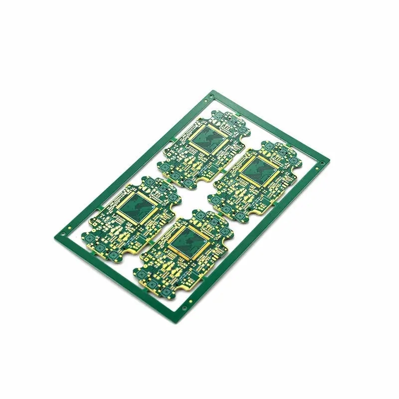
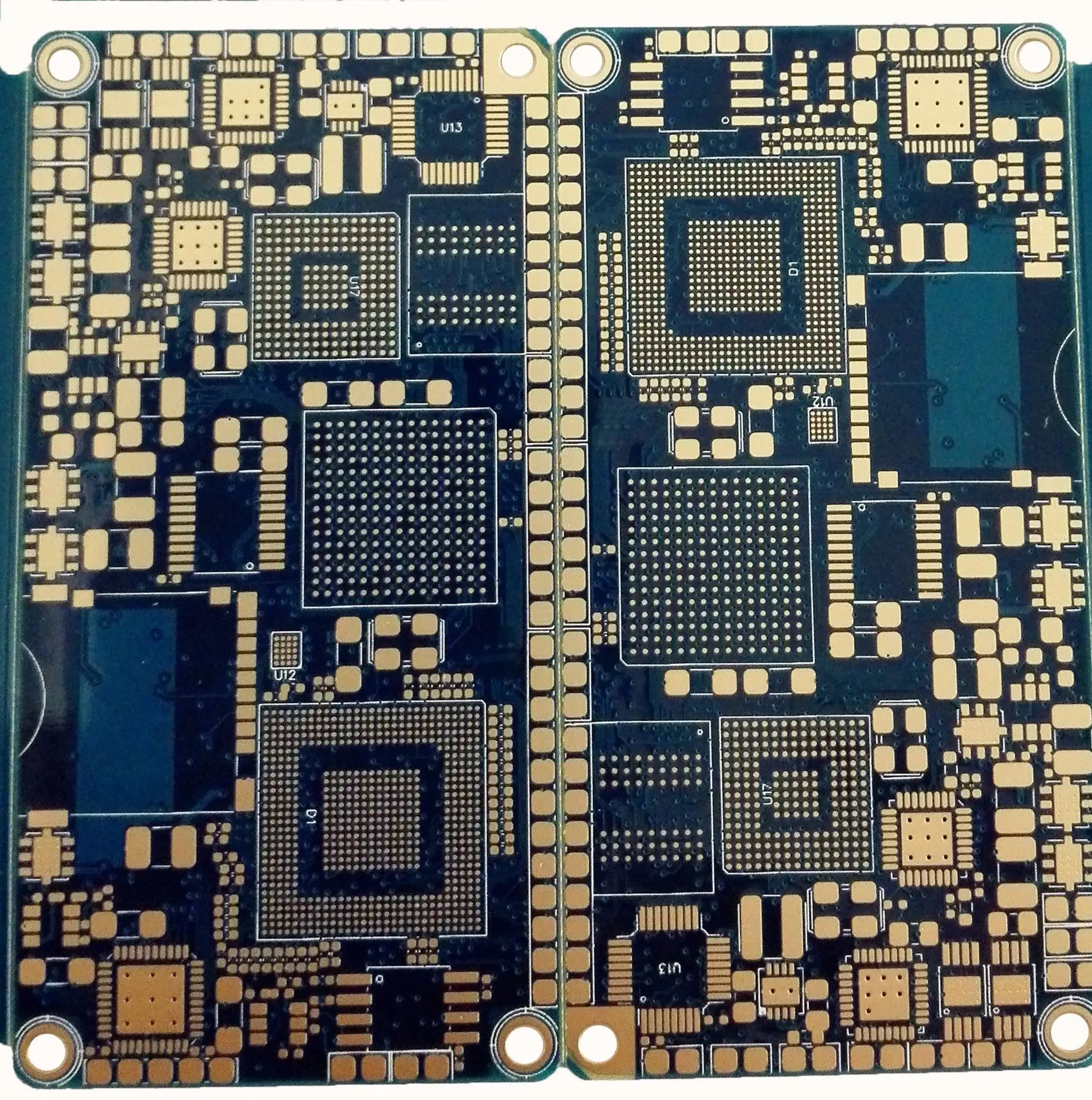
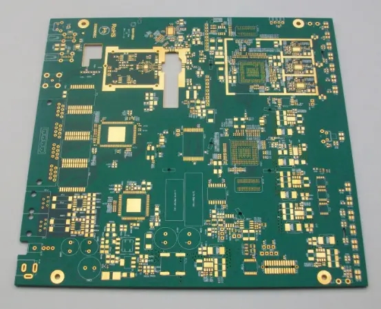
PCB制造
As one of the raw materials for PCB production, how to detect copper foil defects?
Computer aided inspection technology is widely used in industrial production and inspection field. The inspection of finished products and defective products on production lines largely depends on the development of computer image processing technology, such as optICal glass waveform detection, textile detection, weld detection and other applications
Copper foil substrate (CCL) is one of the raw materials for the production of multilayer printed circuit board (PCB). Its product quality seriously affects the quality of PCB, so the quality inspection of copper foil substrate is very important. In the production process, it needs to go through hot pressing, cutting and other processes. Due to equipment and human factors, it may cause damage to the CCL surface and produce various defects. The defects are mainly divided into two categories: scratch and stain. Whether the plate is qualified can be determined according to the type, size and quantity of defects.
Therefore, the inspection of defects is an important aspect of the quality inspection of copper foil substrate products. At present, manual visual inspection is mostly used at home and abroad. This method has strong subjectivity, high miscarriage rate, and the staff is prone to eye fatigue, resulting in reduced detection accuracy. The use of computer technology to achieve intelligent detection will reduce the rate of miscarriage of justice, improve work efficiency, and reduce costs for production enterprises. The detection system proposed in this paper involves optical, electromechanical, computer image processing and other technical fields, and has broad application prOSPects.
1 System composition
The copper foil substrate has a smooth surface and strong light reflection ability. In order to obtain a clear surface image, light sources should be carefully equipped. In this system, several fluorescent lamps are placed above the substrate to generate uniform temperature reflection light, so that the area array CCD CAMera can capture clear target images.
Since the copper foil substrate area is large and the shooting range of one CCD camera is limited, the system sets multiple CCD in the width direction of the substrate according to the coverage range of each camera. In this way, as the substrate moves forward, the CCD camera can capture the entire range of the substrate, so as to analyze and detect the defect image of each part of the substrate.
The image captured by the CCD camera is input to the lower computer through the image acquisition card. The image analysis and processing are completed by the lower computer. The processing results are uploaded to the upper computer for summary, statistics and database storage. At the same time, the upper computer also controls the forward movement of the substrate in real time. The upper and lower computers form Ethernet through the switching mechanism and transmit data through TCP/IP protocol.
Due to the high line speed of the copper foil substrate production line, it reaches the forward speed of 1m/s. The general area array CCD camera adopts the special video transmission standard for image acquisition, transmission and display, and the display is suitable for static image acquisition. If the moving image is captured without any arch, the image will be blurred and difficult to process. In view of the above problems, the system adopts the shutter system equipped with CCD itself and the single frame image acquisition method, that is, only the even field or odd field signals are collected, and then a frame signal is synthesized by interpolation, so as to effectively solve the problem of motion image blur without affecting the processing effect. As the processing object is moving image, the processing speed is required to be high. If color CCD camera and color image acquisition card are used to capture color images, the data volume is large, the system is complex, and the processing speed is slow. For this system, color signal is not required for defect identification, so black and white CCD camera and black and white image acquisition card can be selected to analyze and process gray image, with less data, higher processing speed and cost saving.
2 Image processing
In the process of image acquisition, due to the influence of imaging conditions, uneven lighting, noise caused by photoelectric conversion, pulse interference, error caused by A/D conversion and other factors, the acquired image usually contains noise signals. Therefore, noise filtering is required before image processing. Image smoothing and denoising are mainly realized by neighborhood average method, median filter, frequency domain filter, etc. The system adopts median filtering method, which has the advantages of strong noise removal ability, good boundary details and fast processing speed.
The median filter uses a sliding window with odd points, and replaces the value of the window center point with the median value of each point in the window. Its function is to replace the pixel with a pixel close to the surrounding pixel value which has a large difference with the surrounding pixel gray value, so as to eliminate isolated noise points. It is not SIMple to take the mean value, and it produces less ambiguity. For two-dimensional image data f (i, j), the output fm (I, j) of median filtering is: fM (x, y)=Med {f (i, j)} (1)
Where i and j are in the selected sliding window.
The defects of copper foil substrate are caused by many factors, such as man-made stains, oil drops, waterMARKs, etc., or scratches, folds and other defects during production. In this paper, we take watermark defect as an example to process and recognize the defect image.
In order to extract features and measure parameters of defects, it is first necessary to separate the area where the defects are located from the overall image. There are many methods of region segmentation and extraction in computer image processing, which can be divided into threshold method, edge detection, region growth and other types. The direct use of threshold method for area detection has the advantages of SMAll computation, simple algorithm and fast speed. However, in the case of uneven light intensity and no obvious gray difference between the target and the background, it is difficult to select the threshold. If an appropriate edge detector is used to process the image, the influence of light can be overcome well, and better detection results can be achieved. In this paper, edge detection and threshold method are combined to achieve target extraction.
At present, many effective edge extraction operators have been proposed, such as Sobel operator, Prewitt operator, Lapalas algorithm, Kirsch operator, etc. Sobel edge detection operator is a commonly used gradient operator with low computational cost and easy implementation.
Sobel operator is composed of horizontal and vertical positive templates, which can detect edges in both horizontal and vertical directions. Grayscale image G (x, y) is obtained after Sobel edge detection, that is, edge image. The image contains edge amplitude information. If the output value of the edge detector is less than, it corresponds to the local edge; If the output value is small, it corresponds to an area without edges. Therefore, after edge detection, threshold processing is also required. In this paper, the moment method is used to select the threshold. The experiment shows that the edge area is obvious after two tiMES of Sobel edge detection, which is the image after two times of edge detection and binarization and inversion respectively.
The segmentation of the defect image region provides conditions for morphological feature extraction, but
As can be seen from the image, the boundary has obvious defects, which will seriously affect the accuracy of parameter measurement. Therefore, the mathematical morphology method can be used to compensate the defect contour boundary. In this paper, the closed operation described by formula (5) is adopted, that is, the target is expanded first and then corroded. This method can fill small holes, link adjacent objects, and smooth the boundary without significantly changing the area and status of objects.
PCB manufacturers, PCB designers and PCBA processors will explain how to detect copper foil defects as one of the raw materials for PCB production.


抖音二維碼

Q Q二維碼

微信二維碼
點擊
然后
聯(lián)系
然后
聯(lián)系
電話熱線
13410863085Q Q

微信

- 郵箱