鑫景福致力于滿足“快速服務,零缺陷,輔助研發”PCBA訂購單需求。


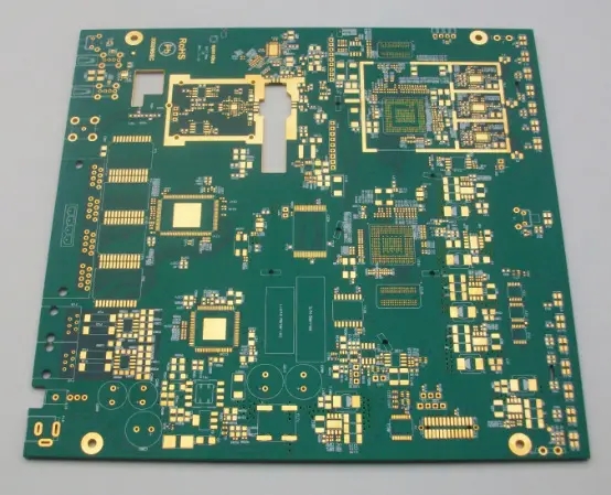
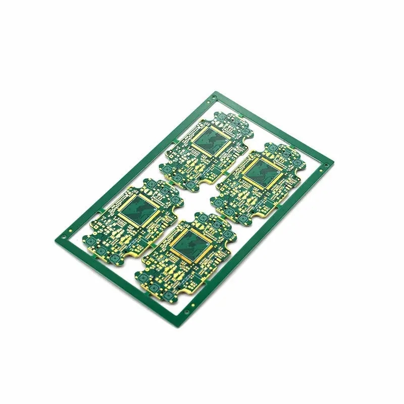
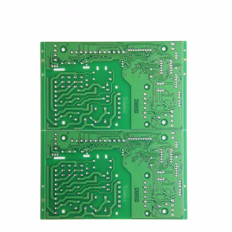
PCB制造
How to solve these problems in PCB production design and production?
In the process of PCB design and fabrICation, engineers need not only to prevent accidents during PCB manufacturing, but also to avoid design errors.
This paper summarizes and analyzes three common PCB problems, hoping to bring some help to everyone's design and production work. There are still many uncommon PCB questions on our website that need to be answered urgently. Are you ready to answer them?
Problem 1: PCB is short circuited
This problem is one of the common faults that directly cause the PCB to fail to work. There are many reasons for this problem. Let's analyze it one by one.
The biggest cause of PCB short circuit is the improper design of the welding pad. At this time, the round welding pad can be changed into an oval, and the distance between points can be increased to prevent short circuit.
Improper design of PCB part direction will also cause board short circuit and failure to work. For example, if the foot of SOIC is parallel to the tin wave, it is easy to cause a short circuit accident. At this time, the direction of the part can be properly modified to make it perpendicular to the tin wave.
There is also a possibility that the short circuit fault of PCB may be caused, that is, the automatic plug-in is bent. As the IPC stipulates that the length of the wire pin is less than 2mm and the parts may fall off if the bending angle is too large, it is easy to cause a short circuit, and the welding spot needs to be more than 2mm away from the line.
In addition to the three reasons mentioned above, there are also some reasons that can lead to the short circuit fault of PCB board, such as too large base plate hole, too low temperature of tin furnace, poor solderability of board surface, solder mask failure, board surface pollution, etc. These are common fault reasons. Engineers can eliminate and check the above reasons and fault conditions one by one.
Problem 2: Dark and granular contacts appear on the PCB
The dark or SMAll granular contact problem on PCB is mostly due to the contamination of solder and the excessive oxide mixed in the dissolved tin, resulting in the brittle solder joint structure. Be careful not to confuse with the dark color caused by the use of soldering tin with low tin content.
Another reason for this problem is that the composition of the soldering tin used in the processing and manufacturing process has changed, and the impurity content is too high, so it is necessary to add pure tin or replace the soldering tin. Physical changes in the fibrous layers of the speckLED glass, such as separation between layers. However, this is not a bad solder joint. The reason is that the substrate is too hot, so it is necessary to reduce the preheating and soldering temperature or increase the substrate travel speed.
Problem 3: PCB solder joints turn golden
Generally, the soldering tin of PCB is silver gray, but occasionally there are golden solder joints. The main reason for this problem is that the temperature is too high. At this time, you only need to lower the temperature of the tin furnace.
Problem 4: Bad boards are also affected by the environment
Due to the structure of the PCB itself, it is easy to cause damage to the PCB under adverse circumstances. Extreme temperature or variable temperature, excessive humidity, high intensity vibration and other conditions are all factors that cause the board performance to be reduced or even scrapped. For example, the change of ambient temperature will cause the deformation of plates. Therefore, the solder joint will be damaged, the shape of the board will be bent, or the copper trace on the board may be broken.
On the other hand, moisture in the air will cause oxidation, corrosion and rust on the metal surface, such as exposed copper traces, solder joints, pads and component leads. Dirt, dust or debris that accumulates on the surfaces of components and circuit boards can also reduce the air flow and cooling of components, causing PCB overheating and performance degradation. Vibration, dropping, striking or bending the PCB will deform it and lead to the cracks, while high current or over-voltage will cause the PCB to be broken down or lead to rapid aging of components and channels.
Problem 5: PCB open circuit
An open circuit occurs when the trace breaks, or when the solder is only on the pad and not on the component lead. In this case, there is no adhesion or connection between the component and PCB. Like short circuits, these can also occur during production or welding and other operations. Vibrating or stretching the circuit board, dropping them or other mechanical deformation factors will damage the trace or solder joint. SIMilarly, chEMIstry or moisture can cause solder or metal parts to wear, resulting in component lead breakage.
Problem 6: Loose or misplaced components
During reflow soldering, the widget may float on the molten solder and eventually leave the target solder joint. The possible causes of displacement or tilt include the vibration or bounce of components on the PCB due to insufficient support of the PCB, reflow furnace setting, solder paste problems, human errors, etc.
Question 7: Welding problems
The following are some problems caused by poor welding practices:
Disturbed solder joint: solder moves before solidification due to external disturbance. This is similar to the cold solder joint, but for different reasons, it can be corrected by reheating, and the solder joint can be free from external interference when cooling.
Cold welding: This happens when the solder cannot be melted correctly, resulting in rough surface and unreliable connection. Cold spots can also occur because excessive solder prevents complete melting. The remedy is to reheat the joint and remove excess solder.
Solder bridge: This occurs when solder crosses and physically connects the two leads together. These may form unexpected connections and short circuits, which may cause the components to be burnt or the wiring to be burnt out when the current is too high.
Pad: insufficient wetting of pins or leads. Too much or too little solder. Pads raised due to overheating or rough welding.
Problem 8: Human error
Most defects in PCB manufacturing are caused by human error. In most cases, the wrong production process, wrong placement of components and unprofessional production and manufacturing specifications lead to up to 64% avoidable product defects. Due to the following reasons, the possibility of defects increases with the complexity of the circuit and the number of production processes: densely packaged components; Multi circuit layer; Fine routing; Surface welded components; Power and ground.
Although every manufacturer or assembler hopes to produce a PCB without defects, there are several problems in the design and production process that cause PCB problems.
Typical problems and results include the following points: poor welding will lead to short circuit, open circuit, cold spot, etc; The dislocation of the plates will lead to poor contact and poor overall performance; Poor copper trace insulation will lead to arc between traces; If the copper trace is too close to the path, the risk of short circuit may easily occur; Insufficient thickness of the circuit board will lead to bending and fracture.
PCB manufacturing, PCB design and PCBA processing manufacturers will explain how to solve these problems in PCB production design and production process.


抖音二維碼

Q Q二維碼

微信二維碼
點擊
然后
聯系
然后
聯系
電話熱線
13410863085Q Q

微信

- 郵箱