鑫景福致力于滿足“快速服務(wù),零缺陷,輔助研發(fā)”PCBA訂購單需求。


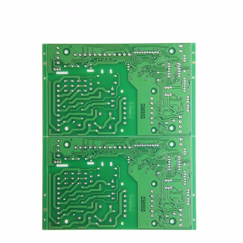
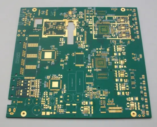
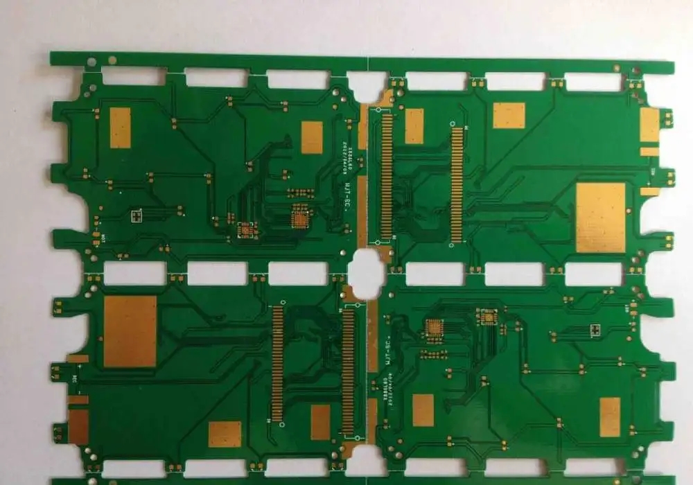
PCB制造
In PCB design, what should we do when encountering problems arising from the substrate?
1、 Various soldering problems
Symptom: there are blasting holes in cold welding points or tin welding points.
Inspection method: analyze the hole frequently before and after immersion welding to find the stress place of copper. In addition, conduct incoming inspection for raw materials.
Possible causes:
1. The blast hole or cold welding point is seen after soldering operation. In many cases, the copper plating is poor, and then the expansion occurs during the soldering operation, resulting in holes or blasting holes on the wall of the metallized hole. If this is generated in the wet processing process, the absorbed volatilization
The object is covered by the coating, and then driven out under the heating effect of immersion welding, whICh will produce a nozzle or a blast hole.
terms of settlement:
Try to eliminate copper stress. The expansion of laminates in the z-axis or thickness direction is usually related to the material. It can promote the fracture of metallized hole. Work with laminate manufacturers to obtain recommendations for materials with low z-axis expansion.
2、 Bond strength problem
Symptom: During the immersion welding process, the bonding pad and the wire are separated.
Inspection method: fully test and carefully control all wet processing processes during incoming inspection.
Possible causes:
The bonding pad or wire separation during processing may be caused by electroplating solution, solvent etching or copper stress during electroplating operation.
2. Punching, drilling or perforating will make the pad partially detached, which will become obvious during hole metallization operation.
3. In the process of wave soldering or manual soldering, the bonding pad or wire separation is usually caused by improper soldering technology or excessive temperature. SometiMES the bonding pad or wire is detached because the laminate is not well bonded or the thermal peeling strength is not high.
4. Sometimes the design and wiring of the printed board will cause the bonding pad or wire to separate at the same place.
5. During soldering operation, the absorbed heat retained by the element will cause the bonding pad to detach.
terms of settlement:
1. Give the laminate manufacturer a complete list of solvents and solutions used, including the processing time and temperature of each step. Analyze whether copper stress and excessive thermal shock occur in electroplating process.
2. Follow the mechanical processing method of pushing. The problem can be controlLED by frequent analysis of metallized holes.
3. Most of the bonding pads or wires are detached due to lax requirements for all operators. If the temperature inspection of the solder pot fails or the dwell time in the solder pot is prolonged, the solder pot will also disengage. In the manual tinning and trimming operation, the pad separation is probably due to improper wattage
Electric ferrochrome and failure to carry out professional process training. Now some laminate manufacturers, for strict tin welding use, have manufactured laminates with high peel strength at high temperatures.
4. If the separation caused by the design wiring of the printed board occurs at the same place on each board; Then this kind of printed board must be redesigned. Usually, this does happen at right angles to thick copper foil or wires. Sometimes, such a phenomenon also happens to long conductors; This is because
Because of the different coefficient of thermal expansion.
5 PCB design When possible, remove the heavy components from the whole printed board or install them after the immersion welding operation. Usually, a low wattage electric soldering iron is used for careful soldering. Compared with component immersion soldering, the substrate material is heated for a shorter duration.
3、 Excessive size change
Symptom: after processing or soldering, the size of the base material exceeds the tolerance or cannot be aligned.
Inspection method: fully control the quality during processing.
Possible causes:
The texture direction of paper-based materials is not paid attention to, and the forward expansion is about half of the horizontal expansion. Moreover, the substrate cannot be restored to its original size after cooling.
2. If the local stress in the laminate is not released, it will sometimes cause irregular size changes during processing.
terms of settlement:
Instruct all production personnel to cut the plates in the same texture direction. If the size change exceeds the allowable range, the base material can be used instead.
2. Contact the laminate manufacturer for advice on how to release the material stress before processing.
PCB manufacturers, PCB designers, and PCBA manufacturers explain to you what to do if you encounter problems in PCB design?


抖音二維碼

Q Q二維碼

微信二維碼
點(diǎn)擊
然后
聯(lián)系
然后
聯(lián)系
電話熱線
13410863085Q Q

微信

- 郵箱