鑫景福致力于滿足“快速服務,零缺陷,輔助研發”PCBA訂購單需求。


PCB制造
What kind of PCB design is very powerful?
Let's briefly describe that the circuit board is designed
1 The first is selection, that is, to select the electronIC components used in our circuit board.
There are many types of electronIC components. Common ones are resistors, capacitors, integrated circuits, etc. There are various types of electronic components with withstand voltage and various packages. When designing a circuit board, we must first select the electronic components that should be placed on the circuit board. Equipment, components or patch electronic components, etc.
2. After selecting the model of each electronic component, the circuit schematic can be designed.
Scheme design needs to use some common scheme design software, such as orCAD. In fact, each schematIC design software is SIMilar, with the same steps and methods. Let you know the simple steps of schematic design.
(1) Open orCAD design software, click File, select New, and select Project to create a project file, as shown in the figure. The project file is created successfully.
(2) For the component package not in the schematic library, first click File, select New, select Library, and then place the corresponding pin according to the electronic component table to create the schematic library.
(3.) Call the package library from the component library provided with the software, place the component symbol in the appropriate position in the schematic drawing area, click [Place], and then click [Part] to place the component.
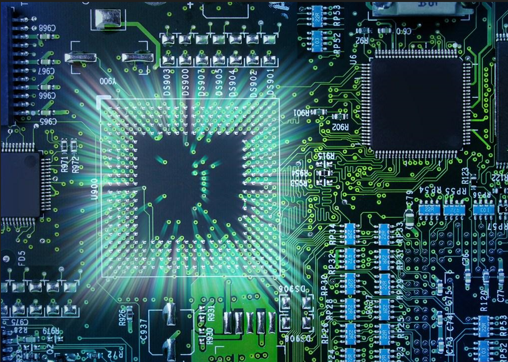
Circuit board

(4) Connect the components with wires to form a loop between them.
USB to TTL
Finally, add packaging information to each component to complete the schematic design process. After the schematic design is completed, one is given. Generate the asc netlist file. The schematic diagram aims to obtain the netlist file. The netlist file is a bridge between various components of PCB, which is very important and relates to the success or failure of the design.
3. PCB design (PrintedCircuit board, meaning printed circuit board). The final PCB design can complete the whole circuit board design process.
PCB design can be roughly divided into five steps: component package library design, component layout, wiring, optimization, and DRC inspection The following is a simple PCB file that has been designed. The relevant information of the design file can be sent to the PCB factory to help us carry out this operation
Single board PCB
The circuit board to be sent by PCB is empty, that is, no electronic components are connected. At this time, we need to weld the electronic components to the empty circuit board by ourselves or the factory to complete the production of the circuit board.
Next, let's look at how to connect circuit Board Designs.
1. If the designed circuit system contains FPGA devices, you must use the Quartus II software to verify the pin assignment before drawing the schematic diagram. (Some special pins in FPGA cannot be used as ordinary IO)
2. The four layers of boards from top to bottom are: signal plane layer, ground, power supply, signal plane layer; From top to bottom, six layers of boards are: signal plane layer, ground, signal inner electric layer, signal inner electric layer, power supply and signal plane layer. For circuit boards with 6 or more layers (advantage: anti-interference radiation), the internal power layer wiring is preferred, and it is not allowed to enter the plane layer. It is prohibited to wire from the ground or the power layer (reason: the power layer will be divided, resulting in parasitic effects).
3. Multi power system wiring: If FPGA+DSP System is used as a 6-layer board, it usually has at least 3.3V+1.2V+1.8V+5V.
3.3V is usually the main power supply. The power layer is directly laid, and the global power network is easily wired through the vias.
5V is usually a power input and only a SMAll amount of copper is required. Try to be thicker (you ask me how thick it should be, the thicker the better)
1.2V and 1.8V are core power supplies (if wiring conduit is directly used, it will be very difficult to face BGA equipment). The 1.2V and 1.8V shall be separated as far as possible during layout, so that 1.2V or 1.8V can be connected. The elements are arranged in a compact area and connected by copper
In short, since the power supply network is distributed on the entire PCB, it will be very complex and time-consuming if wiring is carried out. The method of laying copper is a good choice!
4. The wiring between adjacent layers adopts cross pipes: it can reduce electromagnetic interference (high and medium) between parallel lines and facilitate wiring (refer to 1). The following figure shows the tracks of two adjacent layers in a PCB, which are roughly horizontal and vertical.
5. What is the isolation method between analog and digital isolation? In the layout process, separate the equipment used for analog signal from the equipment used for digital signal, and then cut it from the ad chip!
The analog signal is laid together with the analog grounding, and the analog grounding/analog power supply and digital power supply are connected at a single point through inductor/magnetic bead.
6. PCB design based on PCB design software can also be seen as a software development process. Software engineering focuses on the idea of "iterative computing development". I think this idea can also be introduced into PCB design to reduce the probability of PCB errors.
(1) Check the schematic diagram, pay special attention to the power supply and grounding of the device (the power supply and grounding are the blood of the system and should not be neglected)
(2) PCB packaging diagram (confirm whether the pins in the schematic diagram are wrong)
(3) After confirming PCB package sizes one by one, add verification labels and add them to the package library of this design
(4) Import the netlist and adjust the signal sequence in the schematic diagram during layout (OrCAD component automatic numbering function cannot be used after layout)
(5) Manual wiring (check the power grounding grid while laying the cloth, as mentioned above: the power grid uses copper conduit, so there is less wiring)
In short, the guiding principle of PCB design is to draw and correct the schematic diagram of packaging layout when drawing (considering the correctness of signal connection and the convenience of signal wiring).
7. The crystal oscillator shall be as close to the chip as possible, and no wiring shall be laid below the crystal oscillator, and network copper sheet shall be laid. Clocks used in many places are connected to a tree like clock tree.
8. The arrangement of signals on the connector has a great impact on the difficulty of wiring. When wiring, it is necessary to adjust the signals on the schematic diagram (but do not renumber the components)
9. Multi board connector design:
(1) Use flat cable connection: the upper and lower interfaces are the same
(2) Straight socket: upper and lower interfaces are mirror symmetrical
10. Module connection signal design:
(1) If two modules are placed on the same side of the PCB, it is shown as follows: the serial number of the control system connects the small module to the large module (mirror connection signal)
(2) If two modules are placed on different sides of the PCB, the smaller serial number will be connected to the smaller one, and the larger one will be connected to the larger one.
11. This PCB is designed for power grounding circuit: through improvement, the power supply and ground wire are close to the wiring, which reduces the loop area and reduces electrical interaction (679/12.8, about 54 tiMES) This refore, power and grounding should be as close to the track as possible! The signal line should be avoided as far as possible to reduce mutual inductance between signals


抖音二維碼

Q Q二維碼

微信二維碼
點擊
然后
聯系
然后
聯系
電話熱線
13410863085Q Q

微信

- 郵箱