鑫景福致力于滿足“快速服務,零缺陷,輔助研發”PCBA訂購單需求。


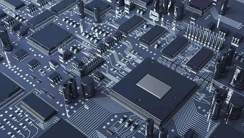
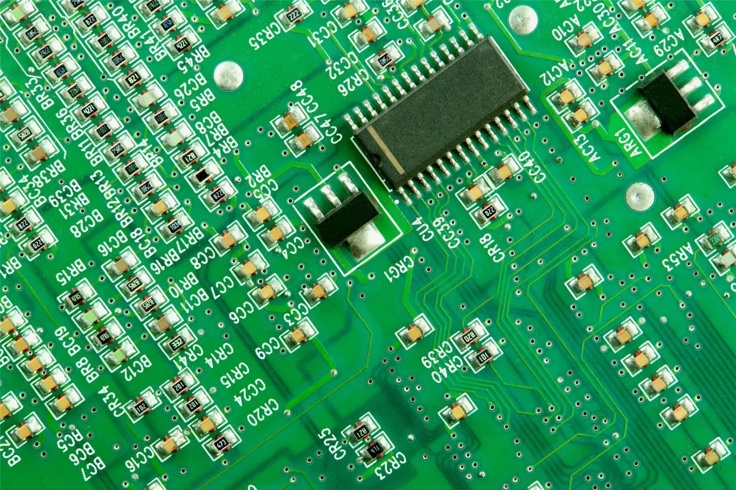
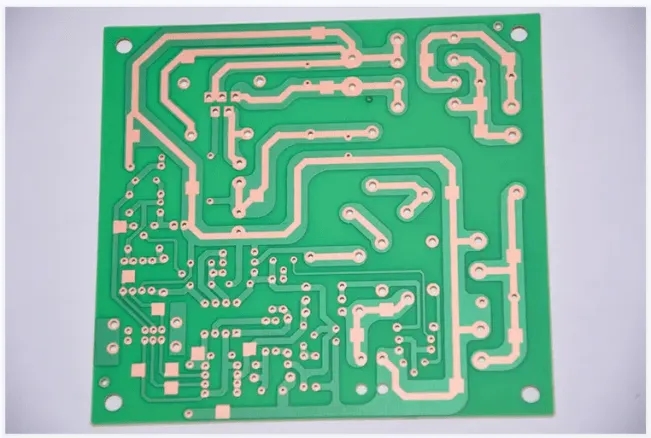
PCB制造
What PCB back drilling technology and instructions before proofing
PCB manufacturing, PCB design and PCBA processing manufacturers explain what PCB back drilling technology is and what matters should be explained before proofing
As all friends who have done PCB design know, PCB via design is very partICular. Today, we will explain the back drilling technology in PCB production in detail.
1. What PCB back drill?
Back drilling is a special kind of deep hole drilling. In the production of multilayer boards, such as the production of 12 layers of boards, we need to connect the first layer to the ninth layer. Usually, we drill through holes (one drill) and then sink copper. In this way, the 1st floor is directly connected to the 12th floor. In fact, we only need to connect the 1st floor to the 9th floor. The 10th floor to the 12th floor are like a pillar because there is no line connecting them; This pillar will cause signal integrity problems and needs to be drilLED off from the opposite side (secondary drilling). So it's called back drill.
2. Advantages of back drilling
1) Reduce noise interference;
2) Improve signal integrity;
3) The local plate thickness becoMES SMAller;
4) Reduce the use of buried blind holes and reduce the difficulty of PCB fabrication.
3. What is the role of back drilling?
The function of back drilling is to drill out the through-hole section without any connection or transmission function, so as to avoid reflection, scattering, delay, etc. of high-speed signal transmission.
4. Working principle of back drilling production
When the drill needle is running in, the micro current generated when the drill needle tip contacts the copper foil on the base plate surface will sense the height of the plate surface, and then run in according to the set running depth, and stop running in when the drilling depth is reached.
5. Backdrill manufacturing process flow
a. The PCB is provided with a positioning hole, which is used for one drill positioning and one drill drilling of the PCB;
b. Electroplate the PCB drilled by one drill, and seal the positioning hole with dry film before electroplating; c. Making the outer layer graphics on the plated PCB;
d. Pattern electroplating is carried out on the PCB after the outer layer pattern is formed;
e. The positioning hole used by one drill is used for back drilling positioning, and the drill cutter is used for back drilling;
f. Water wash the back hole to remove the residual drilling cuttings in the back hole.
6. Application of back drilling plate
The backplane is mainly used in communication equipment, large servers, medical electronics, military, aerOSPace and other fields.
What matters need to be explained to the manufacturer before PCB proofing?
Before PCB proofing, in addition to providing drawings, users need to communicate clearly with PCB manufacturers about their needs, otherwise errors in some small details will directly lead to the scrapping of the entire PCB. Then, what matters should be explained to the manufacturer before PCB proofing?
1. Materials: First of all, we should explain what kind of materials are used. At present, FR4 is the most commonly used, and the main material is epoxy resin peeling fiber cloth board.
2. board layer: The number of layers for making PCB should be stated. The more layers, the more difficult it is to make and the more expensive it is.
3. resistance welding color: There are many colors, which can be selected according to their own requirements. Generally, the most commonly used color is green.
4. Silk screen color: refers to the color of the font and border of silk screen on PCB. Generally, white is preferred.
5. Copper thickness: Generally, the copper thickness will be calculated scientifically according to the current of PCB circuit. Generally, the thicker the copper is, the better, but the cost will be higher, so a reasonable balance is required.
6. Whether the vias are covered with resistance welding: resistance welding is to insulate the vias, otherwise the vias will not be insulated.
7. Surface treatment: common surface treatment processes include tin spraying, gold deposition, gold plating, OSP, hot air leveling, chEMIcal nickel raking, etc; Different surface treatments have different prices and different effects. We must carefully distinguish and inform the manufacturer of the demand.
8. Quantity: The quantity of PCB shall be clearly stated. Some PCB manufacturers specify the minimum quantity, such as 5 pcb or 10 pcb. If this item is not specified, the manufacturer will default to the minimum quantity.
PCB manufacturing, PCB design and PCBA processing manufacturers will explain what PCB back drilling technology is and the instructions before proofing.


抖音二維碼

Q Q二維碼

微信二維碼
點擊
然后
聯系
然后
聯系
電話熱線
13410863085Q Q

微信

- 郵箱