鑫景福致力于滿足“快速服務,零缺陷,輔助研發”PCBA訂購單需求。


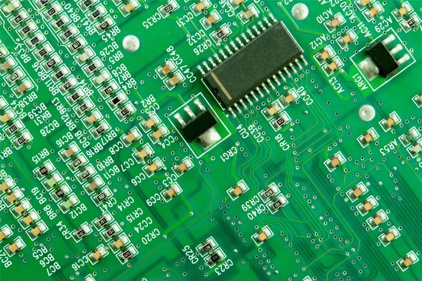
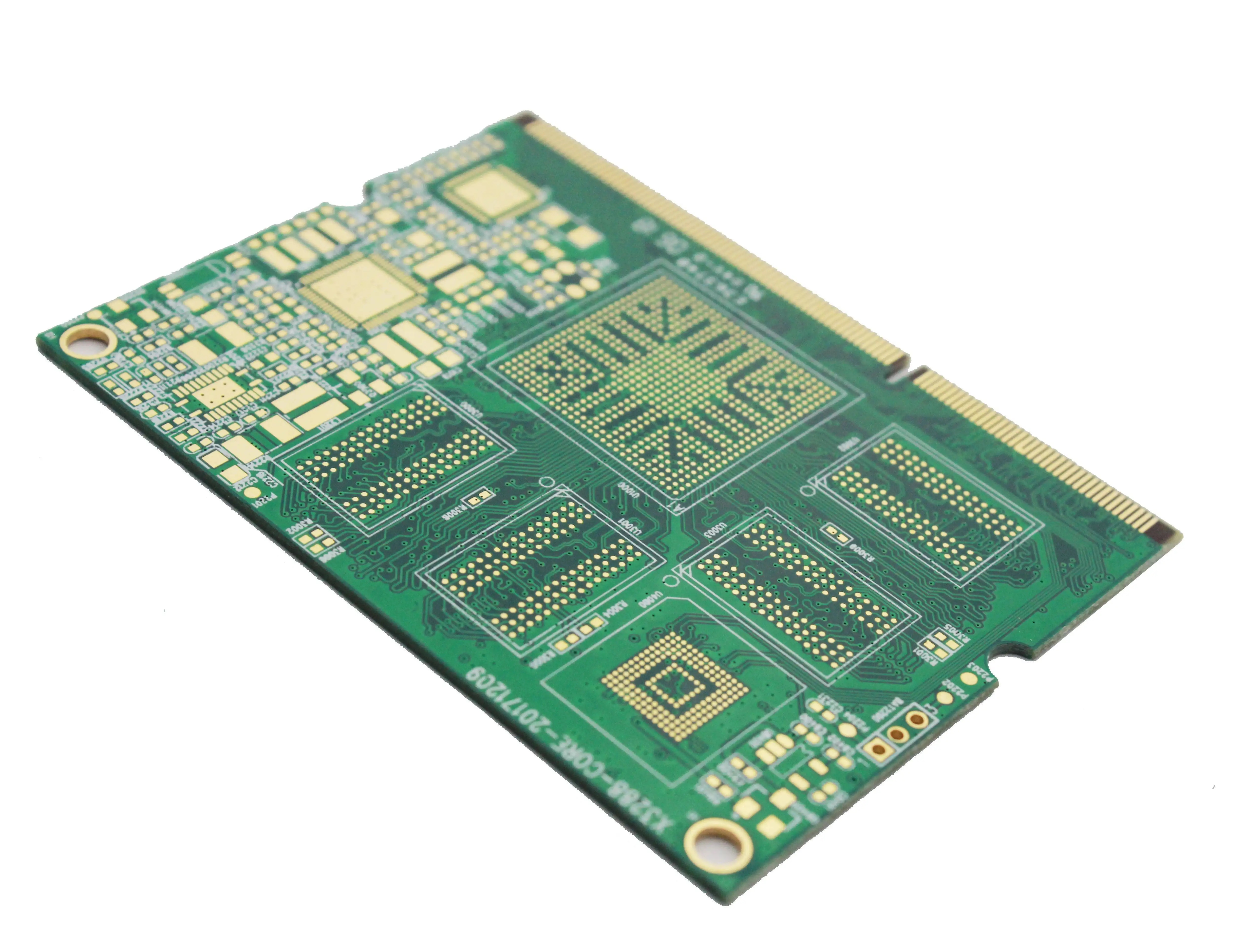
PCB制造
High frequency PCB circuit routing and PCB board selection method
High frequency PCB circuit design is a very complex design process, and its wiring is crucial to the entire design! So, what are the wiring methods of high-frequency PCB circuit?
1. Multilayer board wiring
In the PCB layout stage, reasonably select the size of a certain number of layers of PCB, make full use of the middle layer to set shielding, better realize nearby grounding, effectively reduce parasitIC inductance and shorten the transmission length of the signal, and greatly reduce the cross interference of the signal.
2. The lead between pins of Electronic devices should be bent as little as possible
The lead wire should preferably be a straight line, which needs to be turned. It can use a 45 degree broken line or an arc to turn. Meeting this requirement can reduce the external transmission of high-frequency signals and mutual coupling.
3. The shorter the lead between device pins, the better
The radiation intensity of the signal is proportional to the length of the signal line. The longer the high-frequency signal lead is, the easier it is to be coupLED to the components close to it.
4. The less the lead layer alternation between device pins, the better
It means that the fewer vias (Via) used in the component connection process, the better. Reducing the number of vias can significantly improve the speed and reduce the possibility of data errors.
5. Pay attention to the "crosstalk" introduced by the close parallel routing of signal lines
Since high-frequency signals are transmitted along the transmission line in the form of electromagnetic waves, the signal line will play the role of an antenna, and the energy of the electromagnetic field will be transmitted around the transmission line. The unexpected noise signals generated by the mutual coupling of electromagnetic fields between signals are called crosstalk.
6. High frequency decoupling capacitor is added to the power supply pin
A high-frequency decoupling capacitor is added to the power supply pin of each integrated circuit block nearby, which can effectively suppress the interference caused by high-frequency harmonics on the power supply pin.
7. High frequency digital signal ground wire and analog signal ground wire are isolated
Generally, the ground wire of high-frequency digital signal and the ground wire of analog signal shall be isolated, and the method of single point interconnection at a proper position or high-frequency choke magnetic bead interconnection can be adopted.
8. Avoid loops formed by routing
The routing of various high-frequency signals shall not form a loop as far as possible. If it is unavoidable, the loop area shall be as SMAll as possible.
9. Ensure good signal impedance matching
In the process of signal transmission, when the impedance does not match, the signal will reflect in the transmission channel, which will cause the composite signal to form an overshoot, causing the signal to fluctuate near the logic threshold.
10. Keep the integrity of signal transmission
The integrity of signal transmission shall be maintained to prevent "ground bounce" caused by ground wire division.
What factors need to be considered in PCB board selection?
There are great differences in the scene, product, performance, material, area and other aspects of the use of PCB boards, resulting in great changes in the types of components, thickness of connecting lines, wiring density and other aspects used by different PCB boards. So, what factors should be considered in PCB board selection?
1. For general electronic products, FR4 epoxy glass fiber substrate is used; Polyimide glass fiber substrate shall be used for high ambient temperature or Flexible circuit board; For high-frequency board, PTFE glass fiber substrate is required; For electronic products with high heat dissipation requirements, metal substrate shall be used.
2. The plate with high glass transition temperature (Tg) shall be properly selected, and the Tg value shall be higher than the circuit operating temperature.
3. The plate thermal expansion coefficient (CTE) is required to be low.
4. It is required that the heat resistance of the plate is high. Generally, PCB is required to have heat resistance of 250 ℃/50S.
5. The flatness of the plate is required to be good.
6. In terms of electrical performance, materials with high dielectric constant and low dielectric loss shall be selected for High Frequency Circuit Boards, including insulation resistance, voltage withstand strength and arc resistance.
The above are the factors that should be taken into consideration when selecting PCB boards. I believe that after the customer friends understand this, they can have a definite aim when selecting PCB boards in the future.
PCB manufacturers, PCB designers and PCBA manufacturers will explain the high frequency PCB circuit wiring and PCB board selection methods.


抖音二維碼

Q Q二維碼

微信二維碼
點擊
然后
聯系
然后
聯系
電話熱線
13410863085Q Q

微信

- 郵箱