鑫景福致力于滿足“快速服務(wù),零缺陷,輔助研發(fā)”PCBA訂購單需求。


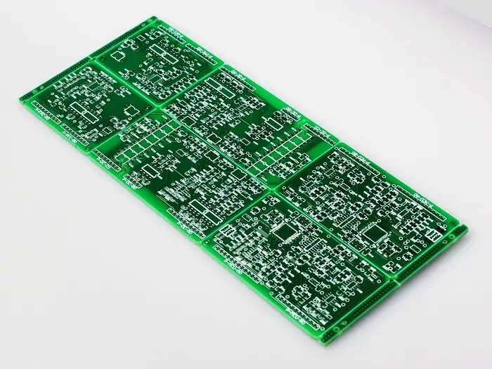
PCB制造
Advantages and Disadvantages of PCB copper Cladding and PCB Heat Dissipation
Copper coating is an important part of PCB design. Whether it is the doMEStIC Qingyuefeng PCB design software, or some overseas Protel, PowerPC B, it provides intelligent copper coating function. So how to apply copper well? I will share some of my ideas with you, hoping to bring benefits to peers.
The so-calLED copper coating is to take the idle space on the PCB as the reference plane, and then fill it with solid copper. These copper areas are also called copper filling. The significance of copper coating is to reduce the ground wire impedance and improve the anti-interference capability; Reduce voltage drop and improve power efficiency; Connecting with the ground wire can also reduce the loop area. In order to keep PCB from deforming as much as possible during welding, most PCB manufacturers also require PCB designers to fill the open area of PCB with copper sheet or grid shaped ground wire. If copper coating is handled improperly, it will be rewarded or lost. Is copper coating "more beneficial than harmful" or "more harmful than beneficial"?
As we all know, the distributed capacitance of the wiring on the printed circuit board will play a role in high frequency. When the length is greater than 1/20 of the corresponding wavelength of the noise frequency, the antenna effect will be generated, and the noise will be EMItted through the wiring. If there is a poorly grounded copper coating in the PCB, the copper coating will become a tool to spread the noise. Therefore, in high frequency circuits, do not think that the ground wire is grounded somewhere, This is the "ground wire", which must be less than λ/ 20, make holes on the wiring, and "well grounded" with the ground plane of the Multilayer board. If the copper coating is properly treated, it not only increases the current, but also plays a dual role in shielding interference.
Generally, there are two basic methods of copper cladding, namely, large-area copper cladding and grid copper cladding. It is often asked whether large-area copper cladding or grid copper cladding is better. Why? Large area copper coating has the dual functions of increasing current and shielding. However, if large area copper coating is used for wave soldering, the board may be warped or even blistered. Therefore, for a large area of copper coating, several grooves are usually opened to alleviate the blistering of copper foil. The SIMple grid copper coating is mainly used for shielding, and the effect of increasing current is reduced. From the perspective of heat dissipation, the grid is beneficial (it reduces the heating surface of copper) and plays a certain role in electromagnetic shielding. However, it should be pointed out that the grid is composed of lines in staggered directions. We know that for circuits, The width of the wiring has its corresponding "electrical length" for the operating frequency of the circuit board (the actual size is divided by the digital frequency corresponding to the operating frequency, see the relevant books for details) When the working frequency is not very high, perhaps the role of grid lines is not very obvious. Once the electrical length matches the working frequency, it is very bad. You will find that the circuit does not work properly at all, and there are signals everywhere that interfere with the work of the system. Therefore, for colleagues who use grid, my suggestion is to choose according to the working conditions of the designed circuit board, instead of holding on to something. Therefore, high-frequency circuit requires high anti-interference multi-purpose grid, and low-frequency circuit has high current circuit and other commonly used complete copper coating.
Having said that, in order to achieve the desired effect in copper cladding, we should pay attention to the following issues in copper cladding:
If there are many PCBs with ground, such as SGND, AGND, GND, etc., the most important "ground" shall be used as the reference for independent copper coating according to the different positions of the PCB board, and the digital and analog copper coating shall be separated. At the same time, before copper coating, the corresponding power supply lines shall be thickened: 5.0V, 3.3V, etc. In this way, multiple deformation structures with different shapes are formed.
2. For the single point connection of different places, the method is to connect through 0 ohm resistance or magnetic bead or inductance;
3. Copper coating near the crystal oscillator. The crystal oscillator in the circuit is a high-frequency emission source. The method is to cover copper around the crystal oscillator, and then ground the shell of the crystal oscillator separately.
4. If the problem of isolated island (dead zone) is too big, it doesn't take much to define and add individual vias.
5. At the beginning of wiring, the ground wire should be treated equally. When wiring, the ground wire should be well laid. It cannot be eliminated as a connected ground pin by adding vias after copper coating. This effect is very bad.
6. It is better not to have sharp corners on the board ("=180 degrees"), because from the electromagnetic point of view, this constitutes a transmitting antenna! For others, it will always have an impact on whether it is big or SMAll. I suggest using the edge of the arc.
7. The open area of the wiring in the middle layer of the multilayer board shall not be covered with copper. Because it is difficult for you to make this copper clad "good grounding"
8. Metal inside the equipment, such as metal radiator, metal reinforcing strip, must be "well grounded".
9. The heat dissipation metal block of the three terminal voltage regulator must be well grounded. The grounding isolation belt near the crystal oscillator must be well grounded. In a word: if the grounding problem of copper coating on PCB is solved properly, it must be "more advantages than disadvantages". It can reduce the return area of the signal line and reduce the external electromagnetic interference of the signal.
What are the factors that affect the heat dissipation of PCB?
The heat generated when electronic equipment is working, so it is very important to conduct heat dissipation treatment on PCB. So, what are the factors that affect the heat dissipation of PCB? Now let's talk to professional PCB engineers:
1、 Factors of PCB board temperature rise
The direct cause of PCB temperature rise is the existence of circuit power consumption devices. Electronic devices have power consumption to varying degrees. The heat intensity varies with the power consumption.
Two phenomena of temperature rise in printed circuit board:
(1) Local temperature rise or large area temperature rise;
(2) Short time temperature rise or long time temperature rise.
2、 When analyzing the factors affecting the heat dissipation of PCB, the following aspects are generally analyzed:
1. Electrical power consumption:
(1) Analyze the power consumption per unit area;
(2) Analyze the distribution of power consumption on PCB.
2. Structure of printed circuit board:
(1) Dimensions of printed boards;
(2) Materials of printed boards.
3. Installation mode of printed circuit board:
(1) Installation mode (such as vertical installation and horizontal installation);
(2) Sealing condition and distance from the casing.
4. Thermal radiation:
(1) Radiation coefficient of printed board surface;
(2) The temperature difference between the printed board and the adjacent surface and their absolute temperature.
5. Heat conduction:
(1) Install the radiator;
(2) Conduction of other mounting structures.
6. Thermal convection:
(1) Natural convection;
(2) Forced cooling convection.
Conclusion: The analysis of the above factors is an effective way to solve the heat dissipation of PCB. Often in a product or system, these factors are interrelated and dependent, and should be analyzed according to the actual situation.
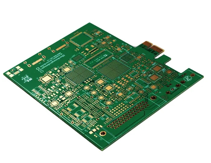
PCB manufacturers, PCB designers and PCBA manufacturers explain the advantages and disadvantages of PCB copper coating and PCB heat dissipation.


抖音二維碼

Q Q二維碼

微信二維碼
點擊
然后
聯(lián)系
然后
聯(lián)系
電話熱線
13410863085Q Q

微信

- 郵箱