鑫景福致力于滿足“快速服務,零缺陷,輔助研發”PCBA訂購單需求。


PCB制造
Why is it more diffICult to produce PCB multilayer boards than single-layer boards
Do you know the difficulties in the production process of PCB multilayer boards? There are many things to pay attention to in PCB design, whether it is design principles or device mix and match, there are strict requirements. So what are the difficulties about the factory process of Multilayer board?
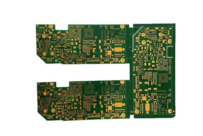
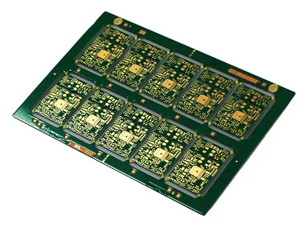
PCB multilayer circuit boards are usually defined as 10-20 or more advanced multilayer circuit boards, which are more difficult to process than traditional multilayer circuit boards, and require high quality and reliability. It is mainly used in communication equipment, high-end servers, medical electronics, aviation, industrial control, military and other fields. In recent years, the MARKet demand for high layer boards in communication, base stations, aviation, military and other fields is still strong.
PCB average level has become an important technical indicator to measure the technical level and product structure of PCB enterprises. This paper briefly describes the main processing difficulties encountered in the production of high-level circuit boards, and introduces the control points of key production processes of multilayer circuit boards for reference.
Compared with traditional PCB products, high layer PCBs have the characteristics of more plate thickness, more layers, dense lines, more through holes, large cell size, thin dielectric layer, etc., and have higher requirements for internal space, inter layer alignment, impedance control and reliability.
1. Difficulties in interlayer alignment
Due to the large number of layers in the high-level panel, users have higher and higher requirements for PCB layer calibration. Generally, the alignment tolerance between layers is controlLED at 75 microns. Considering the large unit size of high-rise boards, the high temperature and humidity of the graphic conversion workshop, the dislocation overlap caused by the inconsistency of different core boards, and the positioning mode between layers, it is more difficult to control the centering of high-rise boards.
2. Difficulties in making internal circuits
High TG, high speed, high frequency, thick copper, thin dielectric layer and other special materials are used for the high layer board, which puts forward high requirements for the internal circuit fabrication and graphic size control. For example, the integrity of impedance signal transmission increases the difficulty of internal circuit manufacturing.
The width and line spacing are SMAll, the open circuit and short circuit increase, the short circuit increases, and the qualification rate is low; There are many thin line signal layers, and the probability of AOI leakage detection in the inner layer increases; The inner core plate is thin, easy to wrinkle, poor exposure, and easy to curl when etching; High level plates are mostly system boards with large unit size and high product scrap cost.
3. Difficulties in compression manufacturing
Many inner core plates and sEMI solidified plates are overlapped, and defects such as sliding plate, delamination, resin void and bubble residue are easy to appear in stamping production. In the design of the laminated structure, the heat resistance, pressure resistance, glue content and dielectric thickness of the material shall be fully considered, and a reasonable pressing scheme for the high-rise plate shall be formulated. Due to the large number of layers, the consistency between expansion and contraction control and size coefficient compensation cannot be maintained, and the interlaminar reliability test is easy to fail due to the thin layer insulation.
4. Difficulties in drilling
The use of high TG, high speed, high frequency, thick copper special plates increases the difficulty of drilling roughness, drilling burr and drilling dirt removal. The number of layers is large, the total copper thickness and plate thickness are accumulated, and the drilling tool is easy to break; CAF failure caused by many dense BGAs and narrow hole wall spacing; Inclined drilling is easy to occur due to the thickness of the plate. These are the difficulties in the production process of PCB multilayer boards
Can the PCB design wiring go at 90 degree right angles?
"PCB design should avoid right angle wiring". Most PCB engineers know this requirement. So, the PCB design wiring must not go at a 90 degree right angle? To answer this question, first understand the influence of 90 ° right angle routing on signals. The influence of 90 ° right angle routing on signals is mainly reflected in three aspects:
1. The right angle can be equivalent to the capacitive load on the transmission line to slow down the rise time;
2. Impedance discontinuity will cause signal reflection;
3. EMI generated by right angle tip.
The reason why 90 ° right angle routing causes signal integrity problems is that the width of the copper foil at the right angle corner of the transmission line is wider than that of the straight line routing, which will cause sudden changes in the characteristic impedance at the right angle bend; This will not cause problems for normal signal routing, but for high-speed transmission lines, it will cause signal reflection, and serious reflection will cause signal integrity problems. Therefore, in the design of high-speed circuit boards, the signal reflection caused by the change of wiring width and the change of signal rise delay caused by this additional discrete capacitance can be reduced by routing in the 45 ° corner mode rather than in the 90 ° corner mode.
In addition, many people think that the right angle tip is easy to transmit or receive electromagnetic waves and generate EMI, which has also become one of the reasons why many people believe that they can not route at right angles.
In general, it is recommended that no right angle is allowed when PCB layout is carried out. Whether it is an ordinary signal line, a high-speed digital signal transmission line, or a RF transmission line, including copper clad copper sheet, it should be designed as an obtuse angle.
PCB manufacturers, PCB designers and PCBA manufacturers explain why it is more difficult to produce PCB multilayer boards than single-layer boards.


抖音二維碼

Q Q二維碼

微信二維碼
點擊
然后
聯系
然后
聯系
電話熱線
13410863085Q Q

微信

- 郵箱