鑫景福致力于滿足“快速服務,零缺陷,輔助研發”PCBA訂購單需求。


PCB制造
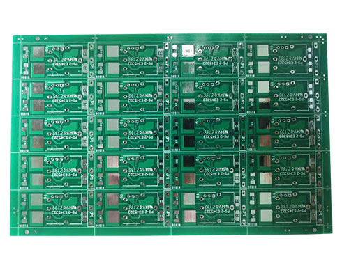
FabrICation and signal integrity of PCBA board component substrate and Copper substrate
circuit board manufacturing, circuit board design and PCBA processing manufacturers will explain the production and signal integrity of PCBA board component substrate and copper substrate
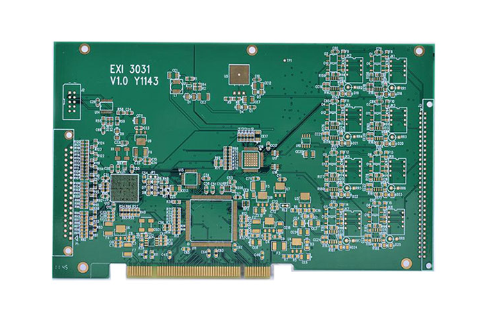
PCBA processing includes the production of circuit boards, PCB proofing, SMT chip processing, component procurement and other processes. What are the selection standards for PCBA board processing components and base materials?
1. Selection of components
The selection of components shall fully consider the needs of the actual area of SMB, and select conventional components as far as possible. Do not blindly pursue SMAll size components to avoid increasing costs. Pay attention to the pin shape and pin spacing of IC devices; QFPs with pin spacing less than 0.5mm should be carefully considered. It is better to directly select BGA packaged devices. In addition, the packaging form of components, PCB solderability, reliability of SMT mounting, and temperature tolerance should be considered.
After selecting components, a component database must be established, including installation dimensions, pin dimensions, SMT manufacturers and other relevant information.
2、 Selection of base materials
The base material shall be selected according to the service conditions and mechanical and electrical performance requirements of SMB. Determine the number of copper-clad foils of the substrate (single side, double side or multiple layers) according to the SMB structure; The thickness of the substrate is determined according to the size of the SMB and the mass of the load-bearing components per unit area. When selecting SMB substrate, factors such as electrical performance requirements, Tg value (glass transition temperature), CTE, flatness, and price should be considered.
What are the problems with PCB signal integrity?
Signal integrity refers to the quality of the signal on the transmission path; With the increase of PCB density, signal integrity has become one of the issues that must be concerned in high-speed digital PCB design. What are the problems with PCB signal integrity?
1. Reflection
When the signal is transmitted on the transmission line, when the characteristic impedance of the uplink transmission line of the high-speed PCB does not match the source impedance or load impedance of the signal, the signal will reflect, causing the signal waveform to overshoot, undershoot and the resulting ringing.
2. Crosstalk
In PCB, crosstalk refers to the undesirable noise interference caused by electromagnetic energy on adjacent transmission lines through mutual capacitance and mutual inductance coupling when signals propagate on transmission lines. It is caused by the interaction of electromagnetic fields caused by different structures in the same area. On a PCB, crosstalk is related to the length of wiring, the distance between signal lines, and the condition of the reference ground plane.
3. Signal delay and timing error
The signal is transmitted at a limited speed on the wire of the PCB. The signal is sent from the drive end to the receiving end, and there is a transmission delay between them. Excessive signal delay or mismatched signal delay may lead to timing errors and confusion of logic device functions.
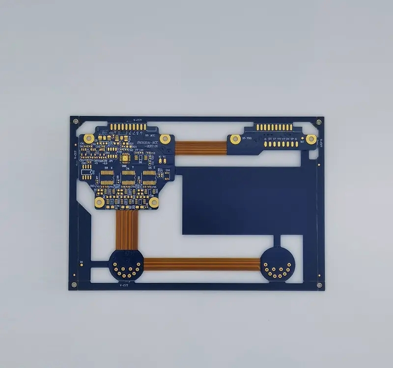
What are the manufacturing processes of PCB copper substrate?
Copper substrate is the most expensive one among metal substrates. Its thermal conductivity is much better than aluminum substrate, and it is suitable for high-frequency circuits; It can be divided into gold plated copper substrate, silver plated copper substrate, tin sprayed copper substrate, oxidation resistant copper substrate, etc; The circuit layer is required to have a large current carrying capacity, so a thicker copper foil is used, with a thickness of 35 μ m~280 μ m。 So, what are the manufacturing process flow of copper substrate? Let's get to know:
1. Cutting: cut the raw material of copper substrate to the size required in production.
2. Drilling: positioning drilling for copper base plate to provide help for subsequent processing.
3. Circuit imaging: display the part required by the circuit on the copper substrate sheet.
4. Etching: After the line is imaged, the required part is retained and the rest unnecessary parts are etched.
5. Silk screen soldering resistance: prevent non soldering points from being contaminated with soldering tin and prevent tin from entering and causing short circuit. During wave soldering, the solder mask is particularly important, which can effectively prevent moisture and protect circuits.
6. Silk screen characters: for MARKing.
7. Surface treatment: protect the surface of copper substrate.
8. CNC: CNC operation of the whole board.
9. Withstand voltage test: test whether the circuit works normally.
10. Packaging and shipment: confirm that the copper base plate is complete and beautiful, and the quantity is correct.
PCB manufacturing, PCB design and PCBA processing manufacturers will explain the production and signal integrity of PCBA board component substrate and copper substrate.


抖音二維碼

Q Q二維碼

微信二維碼
點擊
然后
聯系
然后
聯系
電話熱線
13410863085Q Q

微信

- 郵箱