鑫景福致力于滿足“快速服務,零缺陷,輔助研發”PCBA訂購單需求。


PCB制造
How to distinguish between good and bad colors during PCB proofing
This PCB proofing production PCB equipment judges product quality PCB from PCB color Buyers are always confused about the color of the product PCB, and do not know what color PCB is of high quality Today, I will explain how color affects PCB performance
Pcb proofing production circuit board

First of all, PCB proofreading PCB is used as a PCB, mainly to provide interconnection between electronIC components There is no direct relationship between color and effICiency, and the difference of pigments does not affect electrical efficiency Efficiency PCB is determined by factors such as used (high Q value), wiring design and Multilayer board However, in the cleaning process of PCB, black is the color most likely to cause color difference If the raw materials and manufacturing technology used are slightly different in the PCB factory, the defect rate of the PCB will increase due to color difference This directly leads to new production costs
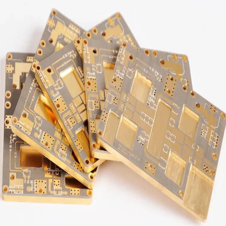
In fact, raw material PCB proofreading PCB can be seen everywhere in our daily life, that is, glass fiber and resin Glass fiber and resin are combined and hardened to form thermal insulation material, insulation, and non flexible board, which is the base of printed circuit board Of course, printed circuit board only made of glass fiber and resin substrate can not transmit signals Therefore, on the PCB substrate, the manufacturer will cover the surface with a layer of copper, so the PCB substrate can also be calLED a copper clad substrate
It will increase the complexity of repair and debugging in the R&D and after sales stages Generally, if there is no brand with strong RD (R&D) person and a strong maintenance team, it is not easy to use black Printed circuit board It can be said that the use of black PCB is a sign of the brand's confidence in the R&D design and post maintenance team From the side, this is also a reflection of the manufacturers' confidence in their own strength
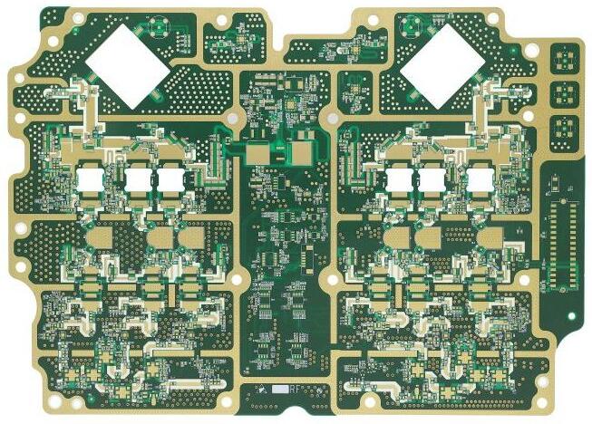
For the above reasons, major manufacturers will carefully consider the design of PCB and their products when selecting Therefore, most of the products with large shipments in the MARKet that year used red PCB, green PCB or blue PCB versions Black printed circuit boards can only be seen on high-end or top flagship products, so customers should not think of black people any more Printed circuit board is better than green printed circuit board
Definition and description of each layer:
1. LAYER (top layer): Designed as the top layer of copper foil wiring If it is a single panel, there is no such layer
2. BOMTTOM LAYER (bottom wiring layer): Designed as bottom copper foil wiring.
3. Top/Bottom solder resist green oil layer: Open the window with a solder mask at the pad, and the vias and non electric traces on the layer
L In the design, the soldering pad will open a window by default (OVERRIDE: 0.1016mm), that is, the bonding pad will expose copper foil and expand 0.1016mm, and tin will be plated during wave soldering It is recommended not to make design changes to ensure solderability;
L The via hole will be opened by default in the design (OVERRIDE: You must check the PENTING option in the additional properties of the vias SOLDER MASK (solver mask opening) to close the via opening if the design is to prevent tin on the vias without exposing copper
L In addition, this layer can also be used separately for non power wiring, and the green oil of the welding mask will correspondingly open the window If it is on the trace of copper foil, it is used to enhance the tracking overcurrent capability, and tin is added during welding; If on the non copper foil trace, it is usually used for logo and special character screen printing, which can save the production of character screen printing layer
4. TOP/BOTTOM PASTE (top/bottom solder paste layer): This layer is generally used to apply solder paste during the SMT reflow process of SMT components, which has nothing to do with the PCB manufacturer's PCB It can be deleted when exporting GERBER, and only the preset value is retained during PCB design
5. TOP/BOTTOM OVERLAY (top/bottom screen printing layer): Designed for various screen printing logos, such as component tag number, role, trademark, etc
6. MECHANICAL LAYERS (mechanical layer): Designed as printed circuit board mechanical shape. The default layer 1 is the shape layer Other floors 2/3/4, etc It can be used for mechanical dimension marking or special purpose For example, when some circuit boards need to be made of conductive carbon oil, the second layer/3/4, etc It can be used, but its purpose must be clearly marked on the same layer
7. KEEPOUT LAYER (forbidden wiring layer): Designed as a forbidden wiring layer. Many designers also use the mechanical appearance of printed circuit boards If there are two printed circuit boards on the platform: No Passage and Mechanical Layer 1, it mainly depends on the integrity of the appearance of these two layers. Generally, Mechanical Layer 1 prevails In design, it is recommended to use mechanical layer 1 as the shape layer If a forbidden layer is used as a shape, do not use mechanical layer 1 to avoid confusion!
8. MIDLAYERS (middle signal layer): most used for multipayer boards It can also be used as a special layer, but its purpose must be clearly marked on the same layer
9. INTERNAL PLANES (internal electrical layer): used for Multi layer boards, our company's design does not use
10. MULTI LAYER (through hole layer): through hole pad layer.
11. DRILL GUIDE (drilling positioning layer): the center positioning coordinate layer of the pad and the hole drilling.
The above is the explanation given by the editor of pcb circuit board company.
If you want to know more about PCBA, you can go to our company's home page to learn about it.
In addition, our company also sells various circuit boards,
High Frequency Circuit Board and SMT chip are waiting for your presence again.


抖音二維碼

Q Q二維碼

微信二維碼
點擊
然后
聯系
然后
聯系
電話熱線
13410863085Q Q

微信

- 郵箱