鑫景福致力于滿足“快速服務(wù),零缺陷,輔助研發(fā)”PCBA訂購單需求。


PCB制造
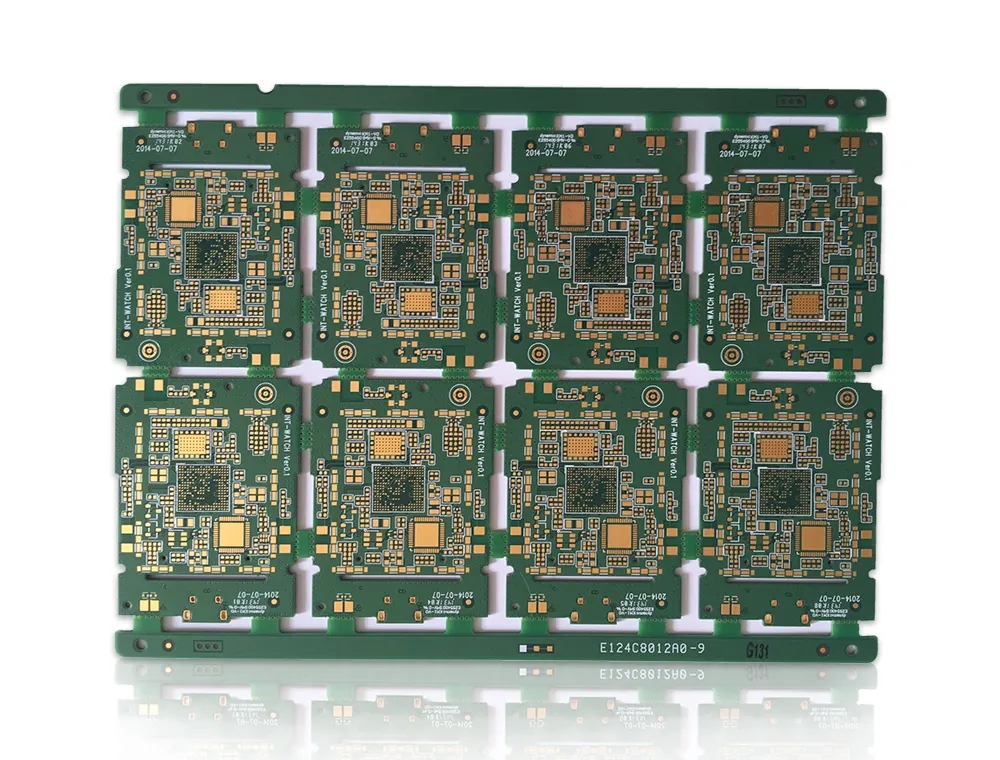
PCB processing manufacturer explains common stack structure of HDI PCB
PCB manufacturers, PCB designers and PCBA manufacturers explain to you the common stacking structures of HDI PCB manufacturers
The SIMple one-time build-up printed circuit board (one-time build-up of six layers of PCB boards, and the stacking structure is (1+4+1)) is the simplest type of board, that is, the inner multilayer circuit board has no embedded holes, and the pressing is completed in one time. Although it is a one-time build-up board, its manufacturing is very similar to the conventional one-time build-up of multilayer circuit boards, but the subsequent difference with multilayer circuit boards is that multiple processes such as laser drilling blind holes are required. Since this laminated structure has no embedded holes, the second and third layers can be used to make a core plate, the fourth and fifth layers can be used as another core plate, the outer layer is added with a medium layer and copper foil, and the middle layer is added with a medium layer and then pressed together at one time. This is very simple, and the cost is lower than that of conventional one-time laminated plates.
2. The structure of conventional primary HDI circuit boards (primary HDI circuit boards have six layers of PCBs, and the stacking structure is (1+4+1)) is (1+N+1), (N ≥ 2, N even number). This structure is the mainstream design of primary HDI circuit boards in the industry. The inner multilayer boards have embedded holes, whICh need to be completed by secondary pressing. This type of primary integrated circuit board has not only blind holes but also embedded holes. If designers can convert this type of HDI circuit board into the first type of simple primary integrated circuit board, it will be beneficial to both the supply and demand sides. After our suggestion, we have many customers who prefer to change the stacking structure of the second type of conventional primary laminate to a simple primary laminate similar to the first type.
3. The conventional secondary HDI circuit board (secondary HDI 8-layer board, stacked structure is (1++1+4+1+1)). The structure of such boards is (1+1+N+1+1), (N ≥ 2, N even number). This structure is the mainstream design of secondary layers in the industry. The inner Multilayer boards have embedded holes, which need three tiMES of pressing. The main reason is that there is no overlapping hole design, and the manufacturing difficulty is normal. If we can change the buried holes of (3-6) layers to those of (2-7) layers as mentioned above, we can reduce one pressing, optimize the process and achieve the effect of reducing costs. This type is like the following example.
4. Another conventional secondary build-up HDI printed board (secondary build-up HDI 8-layer board, the stacking structure is (1+1+4+1+1)). The structure of this type of board (1+1+N+1+1) (N ≥ 2, N even number), although it is a secondary build-up board structure, because the location of the buried hole is not between (3-6) layers, but between (2-7) layers, this design can also reduce the pressing once, so that the secondary build-up HDI boards need three pressing processes, The process is optimized for twice pressing. However, there is another difficulty in making such plates. There are (1-3) layers of blind holes, which are divided into (1-2) layers and (2-3) layers of blind holes. The inner blind holes of (2-3) layers need to be made by filling holes, that is, the inner blind holes of the secondary laminate are made by filling holes. Generally, the HDI cost of the prepared hole filling process is higher than that of the non prepared hole filling process, and the difficulty is also obvious. Therefore, in the design process of conventional secondary laminate, It is recommended not to adopt the overlapping hole design as far as possible, and try to convert (1-3) blind holes into staggered (1-2) blind holes and (2-3) buried (blind) holes. Some experienced designers can adopt this simple design or optimization to reduce the manufacturing cost of their products.
5. Another unconventional secondary layer HDI circuit board (secondary layer HDI 6-layer PCB board, stacked structure is (1+1+2+1+1), It is not allowed to make (1-3) cross layer blind holes into stacked blind holes (1-2) (2-3) blind holes. In addition to the difficulty of laser drilling, the subsequent copper deposition (PTH) and electroplating are also difficult. Generally, PCB manufacturers without a certain level of technology are difficult to make such boards, which are significantly more difficult than conventional secondary laminates. This design is not recommended unless there are special requirements.
6. HDI of secondary stack for blind hole stacking design, and blind hole stacking above buried hole (2-7) layer. (The secondary built-up HDI 8-layer PCB board has a laminated structure of (1+1+4+1+1)). The structure of this type of board is (1+1+N+1+1), (N ≥ 2, N even number). This structure is the current design of some secondary built-up boards in the industry. The inner multilayer boards have embedded holes, which requires secondary pressing. The main feature of this design is that there is a stacked hole design, which replaces the cross layer blind hole design in point 5 above. The main feature of this design is that the blind hole needs to be stacked above the (2-7) buried hole, which makes it more difficult to make. The embedded hole design is in the (2-7) layer, which can reduce a lamination, optimize the process and achieve the effect of reducing costs.
7. The structure of HDI (secondary HDI 8-layer board, laminated structure is (1+1+4+1+1)) with cross layer blind hole design is (1+1+N+1+1), (N ≥ 2, N even number). This structure is a secondary laminated board that is difficult to make in the industry at present. In this design, there are embedded holes in (3-6) layers of the inner multilayer board, which needs three times of pressing. This is mainly due to the cross layer blind hole design, which is difficult to make. HDI PCB manufacturers without certain technical capabilities are difficult to make such secondary laminated boards. If such cross layer blind holes (1-3) are optimally split into (1-2) and (2-3) blind holes, this method of splitting blind holes is not the stacking and splitting method described in points 4 and 6 above, but the splitting method of stagger blind holes, It will greatly reduce the production cost and optimize the production process.
8. The optimization of HDI boards with other laminated structures for three times laminated printed boards or PCB boards with more than three times laminated can also be optimized according to the design concept provided above. For complete HDI boards with three times laminated, the whole production process requires four times of pressing. If you can consider the design idea similar to that of the first or second laminated boards above, you can completely reduce the production process of one time pressing, Thus, the plate forming rate is improved.


抖音二維碼

Q Q二維碼

微信二維碼
點擊
然后
聯(lián)系
然后
聯(lián)系
電話熱線
13410863085Q Q

微信

- 郵箱