鑫景福致力于滿足“快速服務,零缺陷,輔助研發”PCBA訂購單需求。


PCB制造
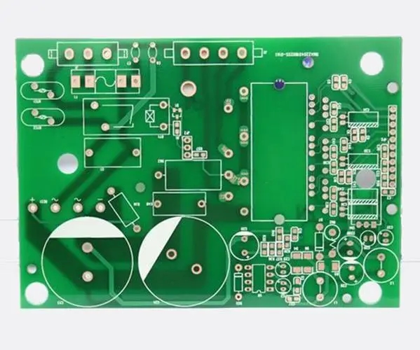
Reasons for Poor PCB quality and the Effect of Large Area Copper Cladding
PCB manufacturers, PCB designers and PCBA processors explain the reasons for poor PCB quality and the role of large-area copper coating
Under the MARKet competition in the circuit board industry, many circuit board factories try to save costs on raw materials and equipment in order to reduce operating costs, whICh ultimately leads to the poor quality of circuit board products. Intellectual creation is Shenzhen PCB Factory. We always take product quality as the driving force for development. Good products are not afraid of good customers. The circuit board editor will share with you the reasons for the poor quality of PCB products.
1. The quality of raw materials for circuit boards is not up to the standard
The quality of PCB raw materials is the basis of PCB quality. If the PCB material itself is not up to the standard, the PCB will bubble. The PCB will be layered, warped, and uneven in thickness.
2. Circuit board production process is not up to standard
Each process of PCB production must be carried out in strict accordance with the production process. At the same time, each process must be equipped with corresponding detection equipment. These process parameters and equipment can ensure the stability of PCB quality. Because the production technology is not up to the standard, many circuit board factories have to lower the price, resulting in the poor quality of the production circuit board.
3. The circuit board production equipment does not meet the standard
With the progress of science and technology, PCB production equipment is being upgraded faster and faster, and the price is becoming more and more expensive. The fundamental way to improve the quality of PCB is to ensure the quality of the equipment from the hardware, increase the investment in the equipment, and make the equipment efficient and stable. As a result, some SMAll PCB manufacturers are unable to purchase expensive equipment, which ultimately leads to the poor quality of PCB proofing products.
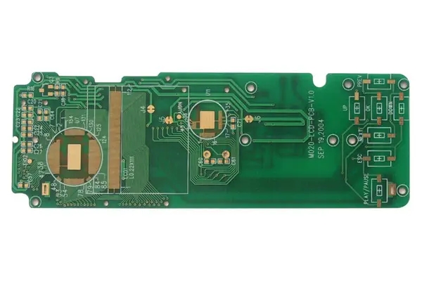
Two functions of large area copper coating on PCB: heat dissipation and anti-interference
PCB circuit boards can be seen everywhere in various applications and instruments. The reliability of circuit boards is an important guarantee to ensure the normal operation of various functions. However, in many circuit boards, we often see that many are large area copper clad, and large area copper clad is used for designing circuit boards.
Generally speaking, large area copper coating has two functions. One is for heat dissipation. As the circuit board current is too high, the power increases. Therefore, in addition to adding necessary cooling elements, such as heat sink, cooling fan, etc., for some circuit boards, it is not enough to rely on these. If it is just for heat dissipation, it is necessary to increase the area of copper foil and also increase the soldering layer, and add tin to enhance heat dissipation.
It is worth noting that due to the large area of copper coating, the bonding degree between PCB and copper foil is reduced due to the long-term heating of the over wave peak or PCB, and the volatile gas accumulated in it cannot be discharged over time. Due to the thermal expansion and cold contraction, the copper foil will expand and fall off. Therefore, if the copper coating area is very large, it is necessary to consider whether there is such a problem. Especially when the temperature is relatively high, it can be windowed or designed as a grid MESh.
The other is to enhance the anti-interference capability of the circuit. As a large area of copper coating can reduce the impedance of the ground wire, it can shield signals to reduce mutual interference. Especially for some high-speed PCB boards, in addition to making the ground wire as thick as possible, the necessary spare places on the circuit board should be grounded, which is "fully grounded". This can effectively reduce parasitic inductance. At the same time, a large area of grounding can effectively reduce noise radiation. For example, for some touch chip circuits, ground wires are paved around each key to reduce the anti-interference ability.
PCB manufacturers, PCB designers and PCBA processors explain the reasons for poor PCB quality and the role of large area copper coating.


抖音二維碼

Q Q二維碼

微信二維碼
點擊
然后
聯系
然后
聯系
電話熱線
13410863085Q Q

微信

- 郵箱