鑫景福致力于滿足“快速服務,零缺陷,輔助研發”PCBA訂購單需求。


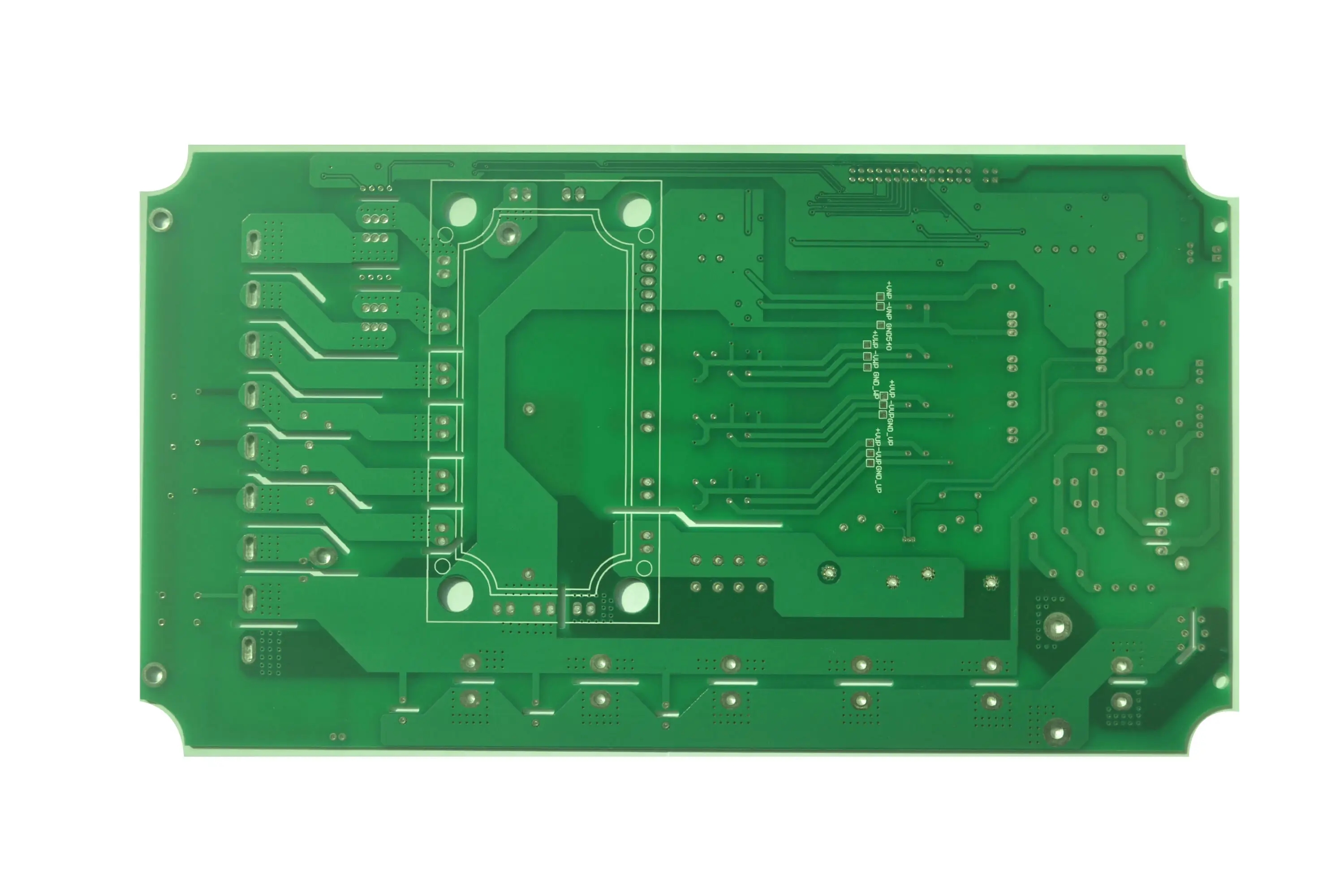
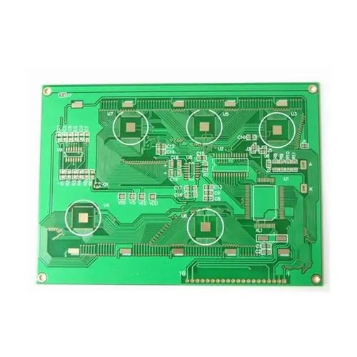
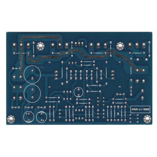
PCB制造
High Frequency Circuit Board applICation, HDI and blind buried orifice
circuit board manufacturers, circuit board designers and PCBA manufacturers will explain the application fields of high-frequency circuit boards and the differences between HDI circuit boards and blind hole boards
High frequency circuit boards refer to special PCB boards with high electromagnetic frequency, which are used in the fields of high frequency (frequency greater than 300 MHz or wavelength less than 1 m) and microwave (frequency greater than 3 GHz or wavelength less than 0.1 m). They are circuit boards produced on the microwave base material copper clad laminate by using part of the process of the common rigid circuit board manufacturing method or using special processing methods. In general, high-frequency circuit boards can be defined as those with frequencies above 1GHz.
With the rapid development of science and technology, more and more equipment are designed for applications in the microwave frequency band (>1GHz) and even in the millimeter wave field (30GHz). This also means that the frequency is getting higher and higher, and the requirements for the substrate of the circuit board are getting higher and higher. For example, the substrate material needs to have excellent electrical properties and good chEMIcal stability. With the increase of power signal frequency, the loss on the substrate is required to be very SMAll, so the importance of high-frequency plates is highlighted.
Application field of PCB high-frequency circuit board
1. Mobile communication products;
2. Power amplifier, low noise amplifier, etc;
3. Power divider, coupler, duplexer, filter and other passive components;
4. Vehicle anti-collision system, satellite system, radio system and other fields.
Difference between HDI board and blind buried hole circuit board
HDI is a product of circuit board, which is calLED highDensityInterconnection. At present, high-order electronic products are generally HDI board products.
Blindvias: Blind holes are vias that connect the inner layer routing of a PCB with the surface layer routing of a PCB. This hole does not penetrate the entire board.
Buried vias: Buried vias only connect the via type of wiring between inner layers, so they cannot be seen from the PCB surface.
With the development of portable product design towards miniaturization and high-density, PCB design is becoming more and more difficult, which puts forward higher requirements for PCB production process. At present, in most portable products, BGA packaging with a spacing of less than 0.65mm has used the design process of blind buried hole, so what is blind buried hole?
Blindvias: Blindvias are vias that connect PCB inner layer routing with PCB surface layer routing. This hole does not penetrate the whole board.
Buried vias: Buried vias only connect the via type of wiring between inner layers, so they cannot be seen from the PCB surface.
The circuit board with buried blind holes is not necessarily HDI circuit board, but generally HDI boards have blind holes, so the buried holes are not necessarily. It depends on the level and pressure of your circuit board product.
The description is as follows:
The first and second order of 6-layer circuit boards are for boards that need laser drilling, namely HDI boards
First order HDI board of 6-layer circuit board refers to blind holes: 1-2,2-5,5-6. That is, 1-2,5-6 needs laser drilling
Second order HDI board of 6-layer circuit board refers to blind holes: 1-2,2-3, 3-4, 4-5, 5-6. That is, two laser drilling is required
First drill 3-4 buried holes, then press 2-5, and then drill 2-3,4-5 laser holes for the first time, then press 1-6 for the second time, and then drill 1-2,5-6 laser holes for the second time. Finally, drill through the hole. It can be seen that the second order HDI plate has been pressed twice and laser drilled twice
In addition, the second order HDI board is also divided into staggered hole second order HDI board and stacked hole second order HDI board. The staggered hole second order HDI board means that the blind holes 1-2 and 2-3 are staggered, while the stacked hole second order HDI board means that the blind holes 1-2 and 2-3 are stacked together, for example: blind: 1-3, 3-4, 4-6
The third and fourth order are the same
Circuit board manufacturers, circuit board designers and PCBA manufacturers will explain the application fields of high-frequency circuit boards and the differences between HDI circuit boards and blind hole boards.


抖音二維碼

Q Q二維碼

微信二維碼
點擊
然后
聯系
然后
聯系
電話熱線
13410863085Q Q

微信

- 郵箱