鑫景福致力于滿足“快速服務(wù),零缺陷,輔助研發(fā)”PCBA訂購單需求。


PCB制造

PCB anti-interference and distinguishing between board electrICity and graphic electricity
PCB manufacturers, PCB designers and PCBA manufacturers explain PCB interference prevention and distinguish between board electronics and graphic electronics
To achieve the best performance of electronic circuits, electronic component circuit boards are the supporting parts of circuit components and devices in electronic products. Even if the circuit schematic is correctly designed and the printed circuit board is improperly designed, the reliability of electronic products will be adversely affected. When designing printed circuit boards, it is important to adopt correct methods, follow the general principles of PCB design, and meet the requirements of anti-interference design. In order to design PCB boards with good quality and low cost, the following general principles should be followed:
First, the size of pcb multilayer circuit board should be considered. When the size of pcb multilayer circuit board is too large, the printed line is long, the impedance increases, the anti noise ability decreases, and the cost increases; If it is too SMAll, the heat dissipation is poor, and adjacent lines are vulnerable to interference. After determining the size of pcb multilayer circuit board, determine the location of special components. Finally, all components of the circuit are arranged according to the functional unit of the circuit.
The following principles shall be observed when determining the location of special electronIC components:
1. The position occupied by the positioning hole and fixing bracket of the printed board shall be reserved.
2. Shorten the connection between high-frequency components as much as possible, and try to reduce their distribution parameters and mutual electromagnetic interference. Components susceptible to interference shall not be too close to each other, and input and output components shall be as far away as possible.
3. There may be high potential difference between some components or wires. The distance between them should be increased to avoid accidental short circuit caused by discharge. Components with high voltage shall be arranged at places where it is not easy to reach during commissioning.
4. Components weighing more than 15g shall be fixed with brackets and then welded. Those large, heavy and heat generating components should not be instalLED on the printed board, but on the chassis backplane of the whole machine, and heat dissipation should be considered. The thermal element shall be far away from the heating element.
5. For the layout of adjustable components such as potentiometers, adjustable inductance coils, variable capacitors, microswitches, etc., the structural requirements of the whole machine shall be considered. If it is adjusted in the machine, it should be placed on the printed board where it is convenient for adjustment; If it is adjusted outside the machine, its position shall be consistent with the position of the adjustment knob on the chassis panel.
The layout of pcb multilayer circuit board for electronic components of the circuit shall meet the requirements of anti-interference design:
Arrange the position of each functional circuit unit according to the circuit flow, so that the layout is convenient for signal flow and the signal is kept in the same direction as far as possible.
2. For circuits operating at high frequencies, the distribution parameters between components should be considered. For general circuits, components shall be arranged in parallel as far as possible. In this way, it is not only beautiful, but also easy to assemble and weld, and easy to mass produce.
3. Take the core components of each functional circuit as the center, and arrange around it. Components shall be uniformly, neatly and compactly arranged on the pcb multilayer circuit board. Try to reduce and shorten the lead wires and connections between components.
4. The electronic components located at the edge of the circuit board are generally not less than 2mm away from the edge of the circuit board. The optimal shape of the circuit board is rectangle. The length and width are 3:2 or 4:3. The size of the circuit board is greater than 200 × For 150mm, the mechanical strength of the circuit board shall be considered.
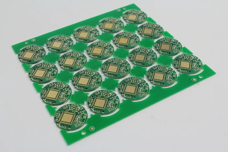
How to distinguish board electricity from graphic electricity
In the PCB circuit board industry, electroplating is used to coat the entire circuit board surface and hole wall with a layer of copper, in order to increase the thickness of the copper layer on the board surface and hole wall of the Circuit board manufacturer, so that it can meet customer requirements.
The figure shows that the outer layer transfers the PCB board to electroplating, followed by secondary copper plating, in order to increase the thickness of the outer layer circuit.
The copper surface attached to the outer dry film cannot be plated with copper or tin; Exposed copper surface.
(The non photosensitive dry film area where the outer development line is dissolved by the development solution) can be plated with secondary copper or tin.
The purpose of tin plating is to protect the copper surface under the tin surface from being bitten off by the etching solution in the next process.
There are two different processes for the production and manufacture of circuit boards: positive and negative. The negative plate passes through the plate electricity after copper deposition. The role of the plate electricity is mainly to increase the thickness of copper on the inner wall of the hole and the thickness of circuit copper on the plate surface to meet the customer's requirements, mainly including micro etching section, pickling section, copper plating section and each water washing section.
There is no difference between a circuit board and a circuit board. They are essentially the same.
A circuit board is just a designed and fabricated base plate. A circuit board is a PCB that has been installed with various components.
The naMES of circuit boards include: circuit board, PCB board, aluminum substrate, high-frequency board, thick copper board, impedance board, multilayer circuit board, multilayer circuit board, PCB, ultra-thin circuit board, ultra-thin circuit board, printed (copper etching technology) circuit board, etc. The circuit board makes the circuit miniature and intuitive, which plays an important role in the mass production of fixed circuits and the optimization of the layout of electrical appliances.
Circuit board: a printed circuit board on an insulating substrate, which is designed to form a point to point connection conductor without printed components.
Circuit board: A printed board on an insulating substrate that is designed to connect wires from point to point and print components.
A circuit board is the one with electronic components, while a circuit board is a PCB without electronic components.
The most contact is the circuit board, and the motherboard is the circuit board.
PCB manufacturers, PCB designers and PCBA manufacturers explain PCB interference prevention and distinguish between board electronics and graphic electronics


抖音二維碼

Q Q二維碼

微信二維碼
點擊
然后
聯(lián)系
然后
聯(lián)系
電話熱線
13410863085Q Q

微信

- 郵箱