鑫景福致力于滿足“快速服務,零缺陷,輔助研發”PCBA訂購單需求。


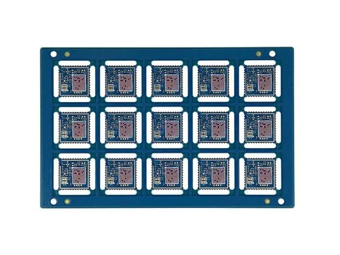
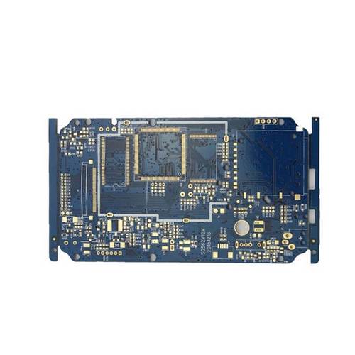
PCB制造
PCB wiring line width and circuit board operation under high temperature
For the setting of PCB wiring line width, two issues should be considered:
One is the current flow. For example, for the power line, it is necessary to consider the current flowing through the circuit during operation. If the current flowing through is large, the wiring should not be too thin.
Measured current carrying capacity of PCB wiring and via
The second is to consider the actual board making capacity of the circuit board factory. If the required current is very SMAll (such as signal wire), you can walk more carefully. SometiMES the PCB area is small and there are many components, so we want to make the wiring as thin as possible, but if it is too thin, the Pcb factory may not be able to make it, or it can not be made, but the defect rate will rise. This can be confirmed with the Circuit board factory. As far as I know, the line width is 0.2mm, and the line spacing is 0.2mm. General circuit board manufacturers can do it. If the line width is 0.127mm, it can not be done. The minimum line width standard in the industry should be 0.1mm. It may be more detaiLED with the development of technology.
As for the size of vias, you can also directly confirm with the circuit board factory. After all, even if you design a PCB with vias with small apertures, the circuit board factory cannot, or can, but the cost is high. As far as I know, the outer diameter is 0.5mm and the inner diameter is 0.3mm, whICh can be done by almost all plate factories.
1. The PCB circuit board needs to make impedance signal lines, which should be set strictly according to the line width and line spacing calculated by the stack. For example, RF signal (conventional 50R control), important single end 50R, differential 90R, differential 100R and other signal lines can be stacked to calculate the specific line width and line spacing.
pcb circuit board needs to be laminated with impedance
2. The design of line width and line spacing should take into account the production process capacity of the selected circuit board factory. If the line width and line spacing set in the design exceeds the manufacturing process capacity of the cooperative PCB manufacturer, it may be necessary to add unnecessary production costs, or it may lead to the design being unable to produce. Normally, the line width and line spacing are controlled to 6/6mil, and the vias are selected to be 12mil (0.3mm). More than 80% of PCB manufacturers can produce, with the lowest production cost. The minimum line width and line spacing are controlled to 4/4mil, and 8mil (0.2mm) is selected for vias. More than 70% of PCB manufacturers can produce them, but the price is slightly more expensive than that of the first case. The minimum line width and line spacing are controlled to 3.5/3.5mil, and 8mil (0.2mm) is selected for vias. At this time, some PCB manufacturers cannot produce, and the price will be more expensive. The minimum line width and line spacing shall be controlled to 2/2mil, and the vias shall be 4mil (0.1mm, usually HDI blind hole design, requiring laser vias). At this time, most PCB manufacturers cannot produce, and the price is the most expensive. The line width and line spacing here refer to the size between line to hole, line to line, line to pad, line to via, hole to plate and other elements when setting rules.
3. Setting rules considers the design bottlenecks in the design file. If there is a 1mm BGA chip, and the pin depth is shallow, only one signal wire is needed between two lines of pins, and 6/6mil can be set. If the pin depth is deep, and two signal wires are needed between two lines of pins, the setting is 4/4mil; There is a 0.65mm BGA chip, which is generally set to 4/4mil; There is a 0.5mm BGA chip. Generally, the minimum line width and line spacing must be set to 3.5/3.5mil; There are 0.4mm BGA chips, and HDI design is generally required. Generally, for the design bottleneck, you can set area rules (see the end of the article for the setting method), set small points for local line width and line spacing, and set larger rules for other parts of the PCB to facilitate production and improve the qualification rate of produced pcbs.
4. It needs to be set according to the density of PCB design. If the density is small and the board is loose, the line width and line spacing can be set a little larger, and vice versa. General can be set according to the following steps:
① 8/8mil, 12mil (0.3mm) for vias.
② 6/6mil, 12mil (0.3mm) for vias.
③ 4/4mil, 8mil (0.2mm) for vias.
④ 3.5/3.5mil, 8mil (0.2mm) for via.
⑤ 3.5/3.5mil, 4mil (0.1mm, laser drilling) is selected for via.
⑥ 2/2mil, 4mil (0.1mm, laser drilling) shall be selected for vias.
The circuit board operates normally at high temperature
The working environment of circuit boards is different, and their materials are required to be different. Some need to work in a low temperature environment, and some need to work in a high temperature environment. This requires that the circuit board materials should be selected according to the actual situation. Today, we will talk about what materials should be used for multilayer PCB circuit boards in a high temperature environment above 100 degrees.
Surface oxidation resistance of double-sided lighting PCB backplane (OSP surface treatment). png
The following is about the circuit board that needs to work at 150 ℃ for a long time. Can it meet the requirements?
When it comes to temperature, we will talk about the selection of Tg value in PCB. First of all, it is Tg value. Tg value refers to the glass transition temperature of CORE. You can understand it as the softening temperature of the board Graded, TG150 of TG in ordinary TG130 is higher than TG170 of TG, and Tg values of FR-4 glass fiber plate used at different temperatures are different, such as:
About 130-140 ℃, the Tg value of common FR-4 glass fiber plate can be used.
The temperature is about 170 ℃, which can use the Tg value of the FR-4 high temperature stair. Generally, when working at this temperature for a long time, the circuit board factory will recommend using the Tg170 value, which has high stability
At the temperature of about 260 ℃, the Tg value of polyimide material shall be used.
With regard to the customer's suggestion of working at 150 ℃ for a long time, the engineer of the circuit board factory suggested that "to ensure the stability of the product, it is recommended to select the beneficial TG170 plate, which can withstand 150 ℃ high temperature for a long time"
The thickness of PCB multilayer board is increased according to customer requirements, and the thickness can be processed. PCB manufacturers, PCB designers and PCBA manufacturers will explain the wiring width of PCB and the operation of PCB under high temperature.


抖音二維碼

Q Q二維碼

微信二維碼
點擊
然后
聯系
然后
聯系
電話熱線
13410863085Q Q

微信

- 郵箱