鑫景福致力于滿足“快速服務,零缺陷,輔助研發”PCBA訂購單需求。


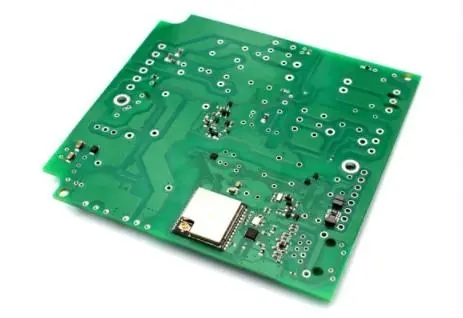
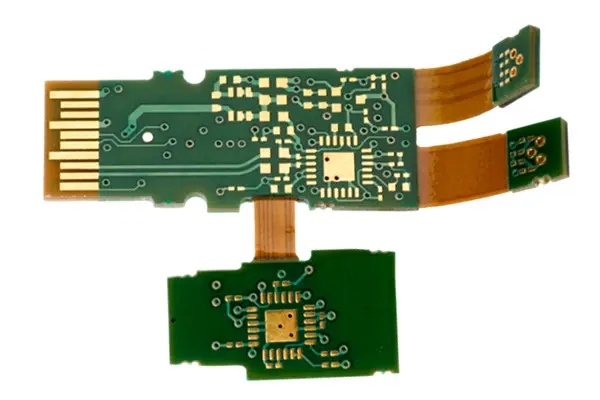
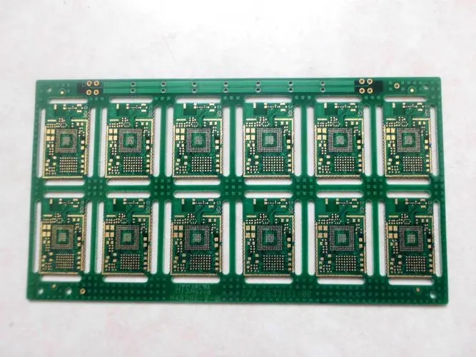
PCB制造
The engineer of the circuit board factory explained: What is CAD?
PCB manufacturers, PCB designers and PCBA manufacturers will explain to you: What is CAD?
In PCB design, there are many different types of CAD software to choose from, including AD, PADS, etc. Although they basICally do the same thing, each CAD program works in a slightly different way, so designers will choose the one that is most suitable for them.
SchematIC design
The PCB design process starts with the technician drawing the component positioning and electrical connection on the circuit board, which is also calLED schematic design. Schematic diagram determines the components in PCB and their connection mode. Designers can use existing schematic design or create their own schematic design. The designer will run the SIMulation to test the schematic diagram as the operation of the actual circuit. This is also one of the main advantages of CAD design; When starting PCB design with hand drawing, there may be some problems that will not be noticed before actually making the circuit.
Convert schematic to circuit layout
After the schematic has been tested and approved, the design must be converted to the actual CAD drawing of the circuit board. Reflect the size of PCB board, placement of components and connection of electrical network. Typically, there is a "Switch to Layout" (or similar) command on the CAD program, and then designers can place components and MARK them with their naMES and values. When designing a schematic, grids are not important, but they become critical when editing an actual board. Select the Move tool to move parts (the operation names are different in different CAD programs), and rotate them to fit your circuit board. Designers will avoid overcrowded component placement or cross routing, as this will lead to short circuits.
When you add multiple circuit board layers, PCB design becomes more complex. Designers usually route one layer horizontally and the next layer vertically, taking into account the physical characteristics of components. The higher one must be placed in some areas, depending on the ultimate use of the circuit board. Components must have complete information required to be part of the board, including drill hole information, pad size, etc.
wiring
This is the stage where designers route the connections between components. The CAD software will route the connections based on the information captured on the schematic. Typically, CAD software will have a "Route" tool to assist with manual routing. However, there are also programs that have automatic routing capabilities. As mentioned above, the crossing of routing must be avoided during wiring. If cross routing is required, the designer will make it cross on the opposite side of the circuit board. Through holes can be used to transfer wiring from one side of the circuit board to the other side. These are holes that are copper coated on the actual circuit. Once all wiring is completed, the CAD program usually provides an option to check the errors in PCB design. Once all errors are corrected, PCB design is completed. Next, PCB Gerber files can be generated for production.
PCB manufacturers, PCB designers and PCBA manufacturers will explain to you: What is CAD?.


抖音二維碼

Q Q二維碼

微信二維碼
點擊
然后
聯系
然后
聯系
電話熱線
13410863085Q Q

微信

- 郵箱