鑫景福致力于滿足“快速服務,零缺陷,輔助研發”PCBA訂購單需求。


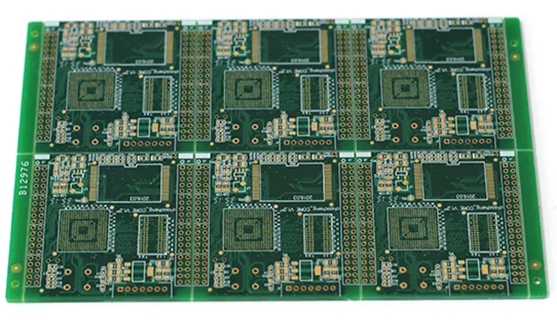
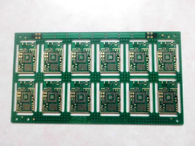
PCB制造
100 PCB people, 99 will make mistakes in these places
The PCB manufacturer, PCB designer and PCBA manufacturer explained 100 PCBs to you, and 99 PCBs would make mistakes in these places
1、 Common errors of schematIC diagram
(1) ERC reports that no signal is connected to the pin:
a. I/O attributes are defined for pins when creating encapsulation;
b. Inconsistent grid attributes are modified when creating or placing components, and pins are not connected to lines;
c. When creating a component, the pin direction is reversed, and it must be connected at the non pin name end.
d. The common reason is that no project file has been created, which is a mistake that beginners are prone to make
(2) Component runs outside the drawing boundary: no component is created in the center of the catalog chart.
(3) The network table of the created project file can only be partially transferred to pcb: global was not selected when generating netlist.
(4) When using components composed of multiple parts created by yourself, never use annotate
2、 Common errors in PCB
(1) NODE is not found when the network is loaded
a. The components in the schematic diagram use packages that are not available in the PCB library;
b. Components in the schematic use packages with inconsistent naMES in the pcb library;
c. Components in the schematic use packages with inconsistent pin numbers in the pcb library. For example, triode: in sch, pin number is e, b, c, while in pcb, it is 1, 2, 3.
(2) Never print on one page when printing
A. When creating the pcb library, it is not at the origin;
b. The components have been moved and rotated for many times, and there are hidden characters outside the boundary of the pcb board. Select Show all hidden characters, shrink the pcb, and then move the characters inside the boundary.
(3) The DRC reporting network is divided into several parts:
This indicates that the network is not connected. Check the report file and select CONNECTED COPPER to find it.
In case of more complicated design, try not to use automatic wiring.
3、 Common errors in PCB manufacturing
(1) Pads overlap
a. It causes heavy holes. When drilling, the drilling is broken and the holes are damaged due to multiple drilling at one place.
b. In a Multilayer board, there are both connecting plates and isolating plates at the same position. The boards are isolated and connected incorrectly.
(2) The use of graphic layer is not standardized
A. It violates the conventional design, such as the component surface is designed at the Bottom layer, and the welding surface is designed at the TOP layer, causing misunderstanding.
b. There are many design wastes on each layer, such as broken lines, useless borders, and labels.
(3) Unreasonable characters
a. Characters cover SMD solder, which brings inconvenience to PCB on-off detection and component welding.
b. The characters are too SMAll, which makes screen printing difficult. The characters overlap each other and are difficult to distinguish. The font is generally>40 mil.
(4) Single side pad set aperture
a. Generally, single side pad does not drill holes, and its hole diameter should be designed as zero, otherwise, when drilling data is generated, the hole coordinates will appear at this location. If drilling, special instructions should be given.
b. If a single-sided pad must be drilLED, but the hole diameter is not designed, the software will treat the pad as a SMT pad when outputting electrical and stratum data, and the inner layer will lose the isolation pad.
(5) Draw pads with filler blocks
In this way, although DRC inspection can be passed, solder resistance data cannot be directly generated during processing, and the pad cannot be welded when covered with solder resistance.
(6) The electrical stratum is designed with both heat sink and signal line. The positive image and negative image graphics are designed together, resulting in errors.
(7) Large area grid spacing is too small
The spacing between grid lines is less than 0.3mm. During PCB manufacturing, the pattern transfer process produces broken film after development, resulting in broken lines, which improves the processing difficulty.
(8) The figure is too close to the outer frame
The spacing shall be at least 0.2mm (more than 0.35mm at V-cut), otherwise the copper foil will be warped and the solder resist will fall off during the appearance processing, which will affect the appearance quality (including the inner copper skin of the multilayer board).
(9) The outline frame design is not clear
Frames are designed for many layers and do not coincide, which makes it difficult for PCB manufacturers to determine which line to use for forming. Standard frames should be designed on the mechanical layer or board layer, and the internal hollowing parts should be clear.
(10) Uneven graphIC design
When the pattern is electroplated, the current distribution is uneven, affecting the uniformity of the coating, and even causing warping.
(11) Short profiled hole
The length/width of the special-shaped hole shall be>2:1, and the width shall be>1.0mm, otherwise the NC drilling machine cannot process it.
(12) Positioning hole of milling profile is not designed
If possible, at least 2 positioning holes with diameter>1.5mm shall be designed in the PCB.
(13) The hole diameter is not clearly MARKed
a. The hole diameter shall be marked in metric system as much as possible and increased by 0.05.
b. Apertures that may be merged shall be merged into one reservoir area as much as possible.
c. Whether the tolerance of metallized holes and special holes (such as crimping holes) is clearly marked.
(14) Unreasonable wiring in the inner layer of multilayer board
a. The heat dissipation pad is placed on the isolation belt, and it is easy to be disconnected after drilling.
b. There is a gap in the design of the isolation belt, which is easy to be misunderstood.
C. The isolation belt is too narrow to accurately judge the network
(15) Design of buried blind orifice
The significance of designing buried blind orifice plate:
a. Increase the density of multilayer boards by more than 30%, reduce the number of layers and reduce the size of multilayer boards
b. Improve PCB performance, especially control of characteristic impedance (wire shortening, aperture reduction)
c. Improve PCB design freedom
d. Reducing raw materials and costs is conducive to environmental protection.
Others have summarized these problems to work habits, and people who have problems often have these bad habits.
Lack of planning
As the saying goes, "If one has no plan in advance, he will find trouble and find it." This also applies to PCB design. One of the many steps for PCB design to succeed is to choose the right tool. Today's PCB design engineers can find many powerful and easy-to-use EDA kits on the market. Each has its own unique capabilities, advantages and limitations. In addition, it should also be noted that no software is foolproof, so problems such as component encapsulation mismatch are bound to occur. It is possible that there is no single tool that can meet all your needs. However, you must study hard in advance to find a better product that is more suitable for your needs. Some information on the Internet can help you get started quickly.
Poor communication
Although the practice of outsourcing PCB design to other manufacturers is becoming more and more common and often very cost-effective, this practice may not be suitable for PCB design with high complexity, because performance and reliability are extremely critical in this design. With the increase of design complexity, in order to ensure accurate component layout and wiring in real time, face-to-face communication between engineers and PCB designers becomes very important. This face-to-face communication will help to eliminate expensive rework in the future.
??
It is also important to invite PCB manufacturers to join in the early stage of the design process. They can provide initial feedback on your design. They can maximize efficiency according to their processes and procedures. In the long run, this will help you save considerable time and money. By letting them know your design goals and inviting them to participate in the early stage of PCB layout, you can avoid any potential problems and shorten the time to market before the product is put into production.
Failure to thoroughly test early prototypes
The prototype board allows you to prove that your design is operating according to the original specifications. Prototype testing allows you to verify the function, quality and performance of PCB before mass production. Successful prototype testing requires a lot of time and experience, but a strong test plan and a clear set of goals can shorten the evaluation time and reduce the possibility of production related errors. If any problem is found during the prototype test, it is necessary to conduct a second test on the reconfigured circuit board. By incorporating high risk factors in the early stages of the design process, you will benefit from multiple iterations of testing, identify any potential problems early, reduce risks, and ensure that the plan can be completed as scheduled.
Use inefficient layout techniques or incorrect components
Smaller, faster devices allow PCB design engineers to design complex layouts. This design will use smaller components to reduce the footprint, and they will also be placed closer together. Using some technologies, such as embedded discrete devices on the internal PCB layer, or ball grid array (BGA) packaging with smaller pin spacing, will help reduce the size of the circuit board, improve performance, and reserve space so that it can be redone after encountering problems. When used with components with high number of pins and smaller spacing, it is important to select the correct PCB layout technology at design time, so as to avoid problems in the future and minimize manufacturing costs.
??
In addition, you must carefully study the value range and performance characteristics of the alternative components you plan to use, even those marked as drop in replacements that can be directly inserted. Minor changes in the characteristics of replacement components may be enough to mess up the performance of the entire design.
Forget to back up your work
Back up important data. Do I need to rEMInd you of this? At least, you should back up your important work achievements and other files that are difficult to replace. Although most companies will back up all the company's data every day, some smaller companies may not do this, or if you work from home, you will not do this. Nowadays, it is so convenient and cheap to back up data to the cloud. There is no excuse not to back up the data and store it in a safe place to avoid theft, fire and other local disasters.
Become a single island
Although you may think that your design is perfect, and making mistakes is not your style at all, many times your peers will see some mistakes in your design that you did not notice. Sometimes, even if you know the complex details of the design, people who have less contact with it may be able to maintain a more objective attitude and provide valuable insights. Reviewing your design frequently with your peers will help you find unforeseen problems, keep your plans on the right track, and keep costs within budget.
Of course, mistakes are inevitable, but as long as you can learn a lesson, you can design a product next time. The PCB manufacturer, PCB designer and PCBA manufacturer explained 100 PCB people to you, and 99 people would make mistakes in these places.


抖音二維碼

Q Q二維碼

微信二維碼
點擊
然后
聯系
然后
聯系
電話熱線
13410863085Q Q

微信

- 郵箱