鑫景福致力于滿足“快速服務(wù),零缺陷,輔助研發(fā)”P(pán)CBA訂購(gòu)單需求。


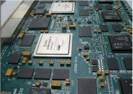
PCB制造
The main function of pcb proofing data converter is either to generate analog waveform by regular time sampling, or to generate a series of regular time sampling by an analog signal. Therefore, the stability of the sampling clock is very important. From the perspective of the data converter, this instability (that is, random clock jitter) will cause uncertainty when the analog to digital converter samples the input signal. In a high-speed system, the timing error of the clock or oscillator waveform will limit the maximum rate of a digital I/O interface. Moreover, it will increase the bit error rate of the communICation link, It even limits the dynamic range of A/D converter (ADC). To obtain the best performance of PCB data converter, it is extremely important to select the sampling encoding clock appropriately.
Pcb proofing ADC circuit
In recent years, the research on high-speed A/D converters abroad has been most active, and some improved structures have appeared on the basic Flash structure [2], such as the sub ranging circuit structure (such as half flash structure, pipelined, multistage structure, multistep structure). In fact, they are circuit structures composed of multiple Flash circuit structures and other functional circuits in different forms. This structure can make up for the defects of the basic Flash circuit structure. It is an excellent circuit design technology to achieve high-speed, high-resolution A/D converters. This structure is gradually replacing the time-honored SAR and integral structures. In addition, there is a class of bit per stage circuit structures, On the basis of it, further improvement will result in a circuit structure calLED Folding (also called Mag Amps structure), which is a Gray code serial output structure. These circuit design technologies have played a positive role in promoting the development of high-speed, high-resolution, high-performance A/D converters.
In addition, in the high resolution A/D converter PCB design technology, Σ-Δ Circuit structure is a very popular circuit design technology at present. This circuit structure will not only gradually replace SAR and integral circuit structures in terms of high-resolution low-speed or medium speed A/D converters, but also combine this structure with pipeline structure, which is expected to achieve higher resolution and higher speed A/D converters.
PCB proofing clock duty cycle stabilization circuit
With the continuous expansion of electronic system functions and the continuous improvement of its performance in the new era of weapons and equipment, the complexity of electronic systems is also increasing. In order to ensure the data sampling, control feedback and digital processing capabilities and performance of electronic systems, modern military electronic systems have increasingly high requirements for A/D converters, especially for military data communication systems, data acquisition systems, high-speed The demand for high-resolution A/D converter is increasing. As the core unit of high-speed and high-precision A/D converter, the clock duty cycle stabilization circuit plays a vital role in the performance of the converter such as SNR and ENOB. Therefore, to ensure the performance of high-speed and high-precision A/D converter, it is necessary to first ensure that the sampling and coding clock has an appropriate duty cycle and very SMAll jitter. Therefore, It is necessary to study the clock duty cycle stabilization circuit.
As the clock duty cycle stabilization circuit is the core unit of high-speed and high-precision A/D converter, and there are few separate clock duty cycle stabilization circuit products, which are only reported in high-speed and high-precision A/D converters. Compared with other companies, ADI's products can improve the sampling performance mainly due to the improvement of DCS (duty cycle stabilizer) circuit, which is responsible for reducing clock signal jitter, The sampling timing depends on the clock signal. The DCS circuits of various companies in the past can only control the jitter at about 0.25ps, while the high-performance new products AD9446 and LTC2208 can reduce the jitter to about 50fs. Generally, reducing the jitter can improve the SNR, so as to improve the effective resolution (ENOB: number of effective bits), and achieve a sampling rate of more than 100Msps while reaching 16 bit quantization bits, If the sampling rate is increased without controlling the jitter, the ENOB will be reduced, and the desired resolution cannot be obtained, nor can the quantization bit be improved. With the development of high-performance A/D converters, the DCS circuit can develop towards higher speed, less jitter and stability. Table 1 lists the main technical and parameter indicators of the clock duty cycle stabilization circuit in overseas A/D converters.
In fact, up to now, the jitter of 60fs of AD Company has been the smallest. Now the aperture jitter is generally controlled at about 1 ps, and jitter higher than this number or even up to dozens of ps is practically meaningless.
Realization of clock stabilization circuit for pcb proofing
From the current research situation at home and abroad, the clock circuit used to stabilize high-speed ADC is mainly a phase locked loop (PLL). In essence, the phase-locked system is a closed loop phase control system. To put it SIMply, it is a circuit that can synchronize the output signal with the input signal in frequency and phase. That is, after the system enters the lock state (or synchronization state), the difference between the output signal of the oscillator and the input signal is zero or constant. Since the phase-locked loop has many excellent characteristics, it can be widely used for clock generation and distribution of high-performance processors Frequency synthesis and transformation of the system, automatic frequency tuning and tracking, bit synchronization extraction in digital communication, phase-locked, phase-locked frequency multiplication and division, etc.
In this paper, a design scheme of delay locked loop (DLL) is proposed. In fact, PLL mainly uses its phase detector and filter to monitor the feedback clock signal and input clock signal, and then uses the generated voltage difference to control the voltage controlled oscillator, so as to generate a signal similar to the input clock, and finally achieve the purpose of frequency locking. The role of DLL is to insert delay pulses between the input clock and the feedback clock, Until the rising edges of the two clocks are aligned and synchronized, the on-chip delay phase-locked loop DLL can be locked only when the input clock edge and the feedback pulse edge are aligned. After the clock is locked, the circuit is no longer adjusted, and there is no difference between the two clocks. In this way, the on-chip delay phase-locked loop uses the DLL output clock to compensate for the time delay caused by the clock distribution network, thus effectively improving the time delay between the clock source and the load. First, compared with the oscillator, the delay line suffers less noise, because the damaged zero crossing point in the waveform disappears at the end of the delay line, and it will be recycled in the oscillator circuit, which will cause more damage. Second, the delay time changes rapidly within the change of the control voltage in the DLL, that is, the transfer function is simply equal to the gain KBCDL of VCDL. In a word, The oscillator used in PLL has instability and phase offset accumulation. Therefore, when the compensation clock causes time delay in the network, the performance of PLL is often reduced. Therefore, the stability and stability speed of DLL are better than those of PLL.
Pcb proofing
◇ Overall circuit structure design of PCB proofing
The overall structure of the clock duty cycle stabilization circuit is shown in the dotted box in Figure 1. It consists of input buffer amplifier A, switches K1, K2 and delay phase-locked loop (DLL).
When the sampling clock frequency is lower than the working lower limit of the DLL, the switches K1 and K2 are closed upward and the DLL is bypassed; When the switches K1 and K2 are closed downward, the DLL starts to work and adjusts the phase of the input clock signal so that the duty cycle of the input clock is close to 50% and the jitter is less than 0.5ps.
◇ pcb proofing delay phase-locked loop (DLL)
The structure of the delay locked loop (DLL) is similar to that of the ordinary phase locked loop (PLL). It only uses the voltage control delay line (VCDL) to replace the voltage controlled oscillator. Its structure block diagram is shown in Figure 2. A common DLL includes four main modules: phase discriminator, charge pump circuit, loop filter and VCDL. The voltage controlled delay line is an open circuit chain composed of a series of voltage controlled delay variable power supplies in series, and its output signal is the delay ntd of the input signal. The input and output of the voltage controlled delay line are sent to the phase discriminator for comparison, and the phase difference between them is locked in one cycle (in-phase comparison) or half a cycle (phase reversal comparison) through the phase lock loop, then the delay time of each delay unit is T/n or T/2n, where n is the number of delay stages.
The function of phase detector in DLL is to identify phase error and adjust the error of charge pump, so as to control the output frequency of voltage oscillator. Common phase detector features cosine type, sawtooth type and triangle type. The phase detector can be divided into analog phase detector and digital phase detector. Its main indicators are:
(1) Phase discrimination characteristic curve. That is, the curve of the output voltage of the phase detector changing with the phase difference of the input signal. This characteristic requires that it be linear and has a large linear range.
(2) Phase discrimination sensitivity. That is, the output voltage generated by unit phase difference, in v/raJ. The phase detection sensitivity of the ideal phase detector shall be independent of the amplitude of the input signal. When the phase detection characteristic is nonlinear, it is generally defined as the sensitivity at Pt=0.
(3) The phase discrimination range is the phase range in which the output voltage varies monotonously with the phase difference.
(4) Operating frequency of phase detector.
The charge pump in DLL is actually a charge switch, which can convert the phase difference, lead and lag into current, and then convert them into control voltage through the integration of the first order capacitor, and then use this feedback control voltage to control the delay time, so as to achieve the required phase delay.
The DLL has two functions: one is to detect the duty cycle; The second is to detect clock jitter. Since the delay phase lock is 50% of the clock cycle, when the phase discriminator (PDF) detects that the duty cycle is greater than 50%, the charge pump (CP) will reduce the duty cycle upward, and vice versa. Professional PCB manufacturers and PCB design solution service providers focus on the development of PCB industry.


抖音二維碼

Q Q二維碼

微信二維碼
點(diǎn)擊
然后
聯(lián)系
然后
聯(lián)系
電話熱線
13410863085Q Q

微信

- 郵箱