鑫景福致力于滿足“快速服務(wù),零缺陷,輔助研發(fā)”PCBA訂購(gòu)單需求。


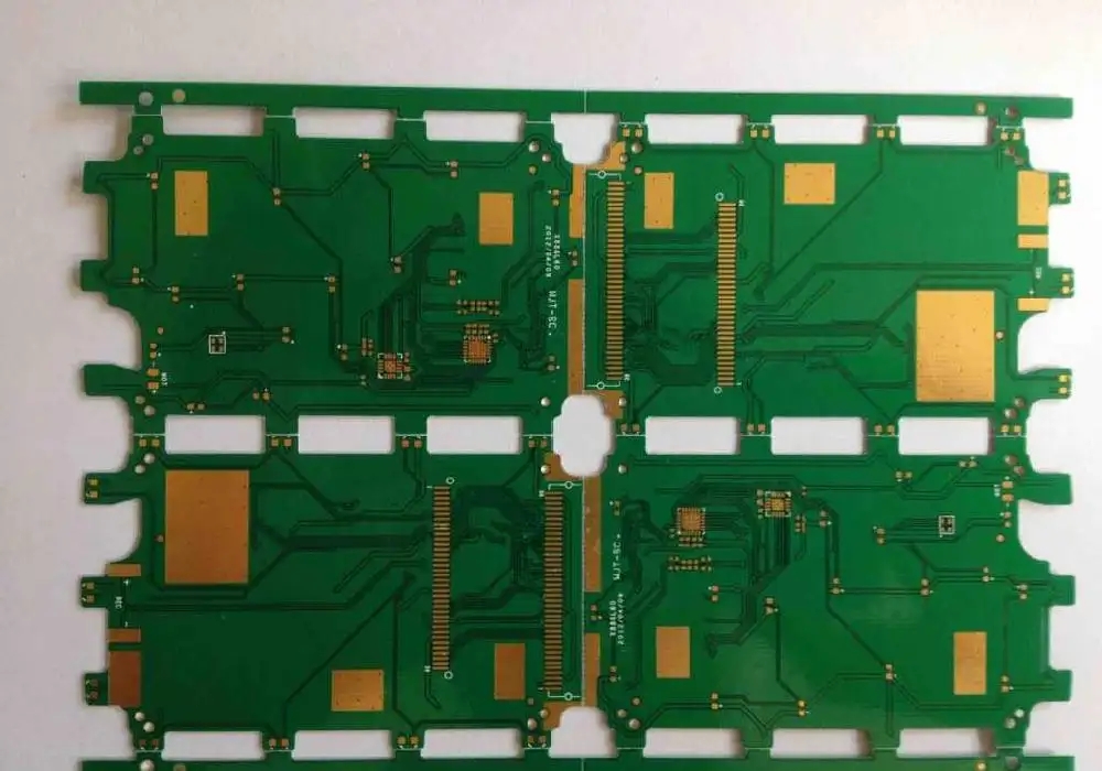
PCB制造
Do you know the advantages of making PCB with even layers?
Do you know that PCB manufacturers, PCB designers, and PCBA manufacturers explain to you the benefits of even layer PCB manufacturing?
designers may design odd numbered printed circuit boards (PCBs). If cabling does not require additional layers, why use it? Won't reducing layers make the board thinner? If the circuit board is one layer less, wouldn't the cost be lower? However, in some cases, adding a layer will reduce the cost.
Structure of circuit board
The circuit board has two different structures: core structure and foil structure.
In the core structure, all conductive layers in the circuit board are laid on the core material; In the foil structure, only the internal conductive layer of the circuit board is applied to the core material, and the external conductive layer is applied to the foil dielectrIC plate. All conductive layers are bonded together by a multilayer lamination process through a dielectric.
Nuclear material is the double-sided foil coating in the factory. Because each core has two sides, the number of conductive layers of PCB is even when it is used in many ways. Why not use foil on one side and nuclear structure on the other? The main reasons are: PCB cost and PCB bending.
Cost advantages of even layer circuit boards
Since there is one less layer of medium and foil, the cost of raw materials for odd PCB is slightly lower than that for even PCB. However, the processing cost of odd PCB is significantly higher than that of even PCB. The processing cost of the inner layer is the same; However, the foil/core structure obviously increases the processing cost of the outer layer.
Non standard laminated core layer bonding process should be added to the core structure process of odd PCB. Compared with the core structure, the production efficiency of the factory adding foil outside the core structure will decrease. Before laminating and bonding, the outer core requires additional process treatment, which increases the risk of outer layer being scratched and etched incorrectly.
Balanced structure to avoid bending
The good reason for not using odd layers to design PCB is that odd layers are easy to bend. When the PCB is cooLED after the multilayer circuit bonding process, the different laminating tensions of the core structure and the foil structure will cause PCB bending when they are cooled. With the increase of PCB thickness, the risk of bending of composite PCB with two different structures is greater. The key to eliminating PCB bending is to use balanced stacking.
Although the bent PCB to some extent meets the specification requirements, the subsequent processing efficiency will be reduced, resulting in increased costs. Because special equipment and process are required during assembly, the accuracy of component placement is reduced, which will damage the quality.
Use Even PCB
When odd PCB layers appear in the design, the following methods can be used to achieve balanced lamination, reduce PCB manufacturing cost, and avoid PCB bending. The following methods are arranged by priority level.
One layer of signal layer is used. This method can be used if the power supply layer of the PCB is even and the signal layer is odd. The added layer does not increase the cost, but it can shorten the delivery time and improve the PCB quality.
Add an additional power layer. This method can be used if the power supply layer of the design PCB is odd and the signal layer is even. A SIMple method is to add a layer in the middle of the stack without changing other settings. First, wire the odd layer PCB, then copy the layer in the middle, and MARK the remaining layers. This is the same as the electrical characteristics of the thickened layer foil.
Add a blank signal layer near the PCB stack center. This method minimizes the stack imbalance and improves the quality of PCB. First, wire according to the odd number of layers, then add a blank signal layer and mark the remaining layers. It is used in microwave circuit and mixed medium circuit (the medium has different dielectric constant).
Advantages of balanced stacked PCB
Low cost, not easy to bend, shorten delivery time, and ensure quality.
Do you know that PCB manufacturers, PCB designers, and PCBA manufacturers explain to you the benefits of even layer PCB manufacturing?


抖音二維碼

Q Q二維碼

微信二維碼
點(diǎn)擊
然后
聯(lián)系
然后
聯(lián)系
電話熱線
13410863085Q Q

微信

- 郵箱