鑫景福致力于滿足“快速服務(wù),零缺陷,輔助研發(fā)”PCBA訂購單需求。


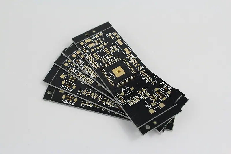
PCB制造
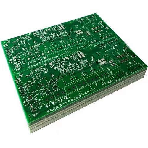
Plate bending, plate warping and pad design of PCB pass back soldering furnace
PCB manufacturers, PCB designers and PCBA manufacturers will explain the bending and warping of PCB through the back soldering furnace and the design of pads
1. Effect of temperature reduction on PCB board stress
Since "temperature" is the main source of plate stress, the occurrence of plate bending and warping can be greatly reduced by reducing the temperature of the reflow furnace or slowing down the heating and cooling speed of the plate in the reflow furnace. However, there may be other side effects, such as solder short circuit.
2. Plate with high Tg
Tg is the glass transition temperature, that is, the temperature at whICh the material changes from glass state to rubber state. The lower the Tg value of the material, the faster the plate begins to soften after entering the reflow furnace, and the longer the time to become soft rubber state will be, of course, the more serious the deformation of the plate will be. The plate with higher Tg can increase its ability to withstand stress and deformation, but the price of materials is relatively high.
3. Increase the thickness of the circuit board
In order to make many electronic products lighter and thinner, the thickness of the board has remained 1.0mm, 0.8mm, or even 0.6mm. It is really difficult to keep the board from deforming in the reflow furnace. It is recommended that if there is no requirement for lightness, the board * can be 1.6mm thick, which can greatly reduce the risk of bending and deformation.
4. Reduce the size of circuit boards and the number of boards
Since most of the reflow furnaces use chains to drive the circuit board forward, the larger the size of the circuit board, the more it will sag and deform in the reflow furnace due to its own weight, so try to put the long side of the circuit board on the chain of the reflow furnace as the board edge, which can reduce the sag and deformation caused by the body weight of the circuit board. This is also the reason to reduce the number of boards, that is, when the furnace is said, The narrow edge shall be perpendicular to the furnace passing direction as far as possible to achieve low sag deformation.
5. Use the furnace tray fixture
If the above methods are difficult to achieve, * it is to use the reflow carrier/template to reduce the deformation. The reason why the reflow carrier/template can reduce the bending warpage is that whether it is thermal expansion or cold contraction, it is hoped that the tray can fix the circuit board until the temperature of the circuit board is lower than the Tg value and the circuit board starts to harden again, and then the round size can be maintained.
If the single-layer tray cannot reduce the deformation of the circuit board, you must add another layer of cover to clamp the circuit board with two layers of trays, which can greatly reduce the deformation of the circuit board through the reflow furnace. However, this tray is very expensive, and it needs to be manually placed and recycLED.
6. Replace V-Cut with Router
Since V-Cut will damage the structural strength of the panels between circuit boards, it is better not to use V-Cut to divide boards or reduce the depth of V-Cut.
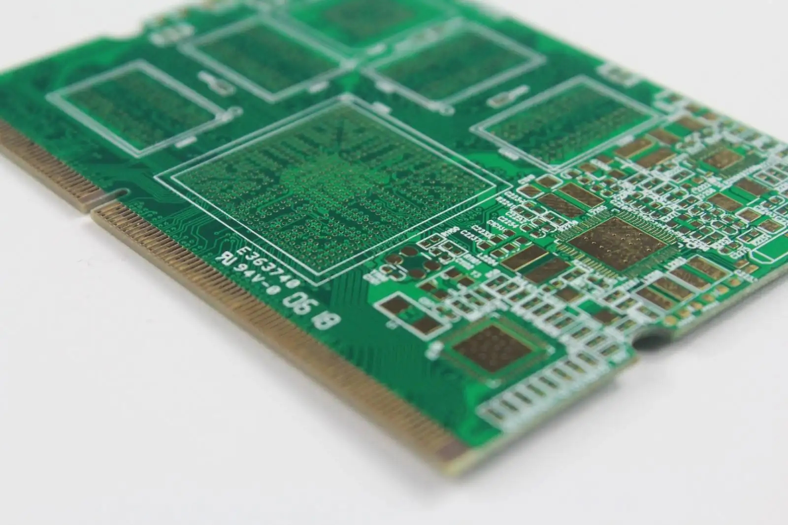
Design of bonding pad in PCB design?
When PCB pads are designed in PCB design, they need to be designed in strict accordance with relevant requirements and standards. Because in SMT chip processing, the design of PCB pad is very important. The pad design will directly affect the solderability, stability and heat transfer of components, as well as the chip processing quality. What is the PCB pad design standard?
1、 PCB pad shape and size design standards:
1. Call PCB standard package library.
2. The minimum single side of the pad shall not be less than 0.25mm, and the maximum diameter of the entire pad shall not be greater than 3 tiMES of the element aperture.
3. Try to ensure that the distance between the edges of two pads is greater than 0.4 mm.
4. Pads with hole diameter more than 1.2mm or pad diameter more than 3.0mm shall be designed as diamond or quincunx pads
5. In case of dense wiring, oval and oblong connecting discs are recommended. The diameter or minimum width of single panel pad is 1.6mm; The hole diameter of the weak current circuit pad of the double-sided board can be increased by 0.5mm, and excessive pad size may cause unnecessary continuous welding.
2、 PCB pad via size standard:
The inner hole of the pad is generally not less than 0.6mm, because it is not easy to process holes SMAller than 0.6mm when punching. Generally, the diameter of the metal pin plus 0.2mm is taken as the inner hole diameter of the pad. For example, when the diameter of the resistance metal pin is 0.5mm, the inner hole diameter of the pad corresponds to 0.7mm, and the diameter of the pad depends on the inner hole diameter.
3、 Key points of PCB pad reliability design:
1. Symmetry: To ensure the balance of the surface tension of molten solder, the pads at both ends must be symmetrical.
2. The space between pads, too large or too small space between pads will cause welding defects, so it is necessary to ensure that the space between component ends or pins and pads is appropriate.
3. The remaining size of the pad, after the component end or pin is lapped with the pad, must ensure that the solder joint can form a meniscus.
4. The width of bonding pad shall be basically consistent with the width of component end or pin.
With correct PCB pad design, if there is a small amount of skew during chip processing, it can be corrected due to the effect of surface tension of molten solder during reflow soldering. If the PCB pad design is not correct, even if the mounting position is very accurate, it is easy to have component position offset, suspension bridge and other welding defects after reflow soldering. Therefore, great attention should be paid to PCB pad design when PCB design is carried out. PCB manufacturers, PCB designers and PCBA manufacturers will explain the bending and warping of PCB through the soldering furnace and the design of pads.


抖音二維碼

Q Q二維碼

微信二維碼
點(diǎn)擊
然后
聯(lián)系
然后
聯(lián)系
電話熱線
13410863085Q Q

微信

- 郵箱