鑫景福致力于滿足“快速服務,零缺陷,輔助研發(fā)”PCBA訂購單需求。


PCB制造
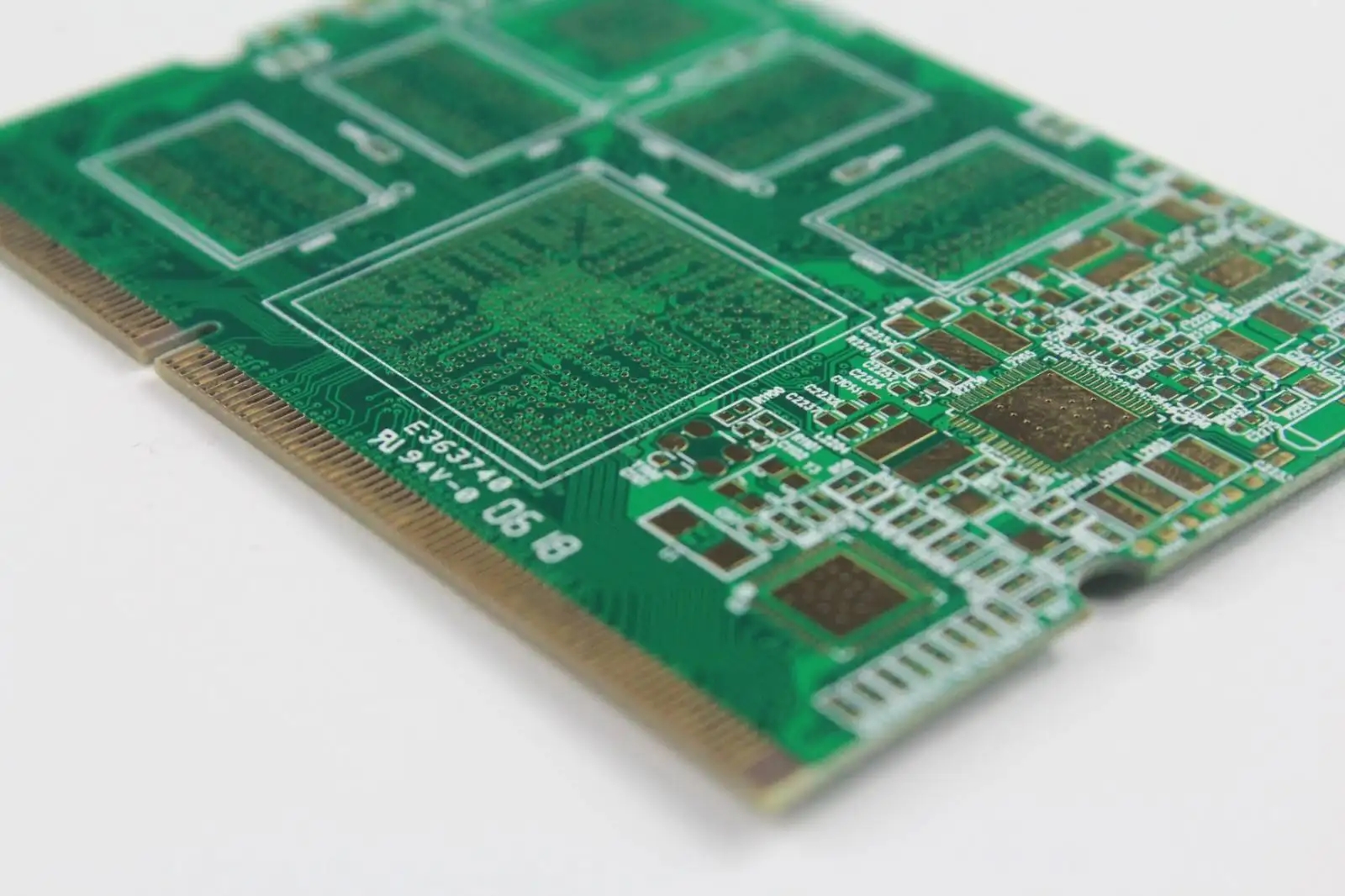
Can you tell the difference between PCB "via oil cover" and "via window"?
circuit board manufacturers, circuit board designers and PCBA manufacturers explain to you the "via oil cover" and "via window opening" of PCBs. Are you stupid?
With regard to "opening windows through holes" and "covering oil through holes" (the usage of PAD and VIA is different), many customers and design engineers often ask what this means when placing orders on the system, and whICh option should I choose for my file?
The following is a description of this problem: we often encounter such problems. The design is seriously non-standard, and we can't tell which is pad, which is the use of via. SometiMES conductive holes are treated with pad attributes, and sometimes keyholes are treated with via attributes. The design of VIA attributes and PAD attributes is confused, which leads to incorrect processing. This is also one of the problems frequently complained about. For circuit board manufacturers, when processing CAM data, Some film processing engineers, because the customer's design documents are not standardized, will make mistakes, help the customer to modify the documents, correct the non-standard design, and process the engineering data based on their own experience, which leads to and encourages the customer's non-standard design. PCB hereby states that: just because you did the right thing last time does not mean your file is right! All engineers must pay attention to the design standards and specifications! PCB will again strictly require all film processing engineers to maintain the status quo of customer documents as much as possible! As far as possible, it should be handLED according to the design specifications and standards, not according to the so-called experience! Show the problems, so that you can give design engineers a reference, improve design quality and reduce problems! This article mainly explains the conductive hole, keyhole, and the connection between protel/pads/and geber files Conductive hole: via Keyhole:
Several problems that are particularly easy to occur with the pad:
1、 Via In the conversion process, the design is not standard or you are not clear about the conversion gerber setting rules, which leads to problems. When you send a gerber file, the manufacturer cannot distinguish between those that are through holes and those that are keyholes. The only thing that can be identified is processing according to the file. If there is a soldering layer, there is a window! Argument point: I asked for a hole covered with oil. Now you open the window for me. I may cause a short circuit. Please check your file. Your gerber is a film file. The factory has no way to check your conductive hole or keyhole. Please check the gerber file. If there is a soldering layer, open the window. If not, cover with oil.
2、 The mixed use of pad and via leads to problems. 1. When your file is pads or protel, it is sent to the factory and requires that the hole be covered with oil. Be careful. You should carefully check whether your plug-in hole (pad) is also useful for via, otherwise your plug-in hole will also be covered with green oil, which leads to no welding dispute points: the plug-in hole must be sprayed with tin, how do you cover the oil, how do I use it, Please check the file when you say this. Is it designed by pad or via! III When your file is protel or pads, send the file to the factory. The order requires that the conductive hole be covered with oil. Many customers use pad (plug-in hole) to represent the conductive hole, which causes your conductive hole to open the window. Maybe you want the conductive hole cover oil. At that time, the point of dispute may be that I want the conductive hole cover oil. Why do you open the window? Please check your file design!
Again, if you are a via, you will be treated as a via, if you are a pad, you will be treated as a pad! Because no one will know that you are a conductive hole, that is a plug-in hole, and via and pad are the only signs, please be clear! 4、 How to design via cap oil in protel or pads—— This is the most standard practice. If the design is standard, there will be no mistakes! There is a tenting option in the via attribute of protel. If it is checked, it must be oil capping. Then all the oil you transfer out is oil capping. In pads, the method of transferring files from pads is to think about hole (via) oil capping: when outputting soldermask, i.e. solder mask, just check the upper soldermask top - the lower via represents all the holes and windows, and if it is not checked, the holes and oil capping
To sum up: the pad is made according to the pad, which is the plug-in hole. Via, you have two choices. If you provide the original file, you can choose it when placing an order. If you provide the gerber file, you must check whether the gerber file meets your requirements! Circuit board manufacturers, circuit board designers and PCBA manufacturers explain to you the "via oil cover" and "via window opening" of PCBs. Are you stupid?


抖音二維碼

Q Q二維碼

微信二維碼
點擊
然后
聯(lián)系
然后
聯(lián)系
電話熱線
13410863085Q Q

微信

- 郵箱