鑫景福致力于滿足“快速服務,零缺陷,輔助研發”PCBA訂購單需求。


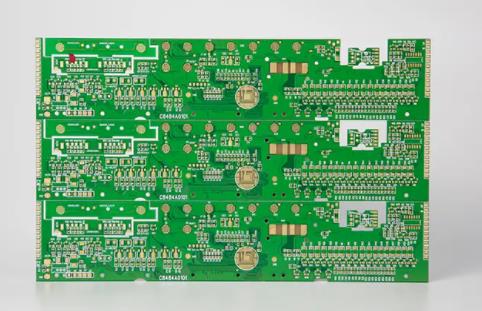
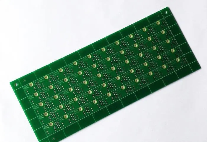
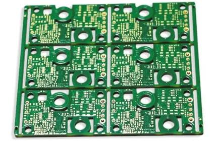
PCB制造
Silver layer defect and control line width and current in PCB production
PCB manufacturers, PCB designers and PCBA manufacturers explain the relationship between silver layer defects in PCB production and pcb design control line width and current
Silver deposition process printing is indispensable in PCB manufacturing, but silver deposition process can also cause defects or scrap.
The formulation of preventive measures needs to consider the contribution of chEMIcals and equipment to various defects in actual production to avoid or eliminate defects and improve the yield.
The prevention of Giavanni effect can be traced back to the copper plating process in the previous process. For high aspect ratio holes and mICro through-holes, uniform plating thickness helps eliminate the hidden danger of Giavanni effect. Excessive corrosion or side corrosion in film stripping, etching and tin stripping process will promote the formation of cracks, and micro etching solution or other solutions will remain in the cracks. In SPIte of this, the problem of solder mask is still the main reason for the Javanni effect. Most of the defective plates with Javanni effect have side erosion or the solder mask falls off. This problem mainly coMES from the exposure development process. Therefore, if the solder mask is "positive foot" after development and the solder mask is completely solidified, the Giavanni effect problem can be almost eliminated.
To get a good silver layer, 100% metal copper must be used at the silver deposition position. Each tank solution has good through-hole capacity, and the solution in the through-hole can be effectively exchanged. If it is a very fine structure, such as HDI board, it is very useful to install ultrasonic wave or injector in pretreatment and silver precipitation bath solution. For the production management of silver deposition process, controlling the micro etching rate to form a smooth and semi bright surface can also improve the Giavanni effect. For original equipment manufacturers (OEMs), the design of connecting large copper surfaces or high aspect ratio through-holes with thin lines should be avoided as far as possible to eliminate the hidden danger of Giavanni effect. For chemical suppliers, the silver precipitation solution should not be very aggressive, and should maintain an appropriate pH value. The silver precipitation speed should be controlLED and the expected crystal structure can be generated to achieve the best corrosion resistance with the thinnest silver thickness.
Corrosion can be reduced by increasing coating density and reducing porosity. Sulfur free materials are used for packaging. At the same time, seals are used to isolate the contact between the board and the air, and prevent the sulfur carried in the air from contacting the silver surface. It is better to store the packed boards in an environment with a temperature of 30 ℃ and a relative humidity of 40%. Although the shelf life of the silver plate is very long, the first in, first out principle should still be followed during storage.
How to control the relationship between line width and current in PCB design?
We generally have a common sense when drawing PCB, that is, thick lines (such as 50mil or above) can be used in places with high current, and thin lines (such as 10mil) can be used for signals with low current.
For some electromechanical control systems, sometimes the instantaneous current flowing through the wiring can reach more than 100A. In this case, the thin wire will definitely have problems.
A basic empirical value is: 10A/mm2, that is, the current value that can safely pass through the wiring with a cross-sectional area of 1 mm2 is 10A. If the wire width is too thin, the wire will be burnt when the large current passes through. Of course, the energy formula should also be followed when the current is burnt out: Q=I * I * t. For example, for a 10 A line, a 100 A current burr suddenly appears, and the duration is US level, then the 30 mil wire can certainly withstand. (Another problem will arise at this time. The stray inductance of the wire will generate a strong reverse electromotive force under the effect of this inductance, which may damage other devices. The thinner and longer the wire is, the larger the stray inductance is, so the actual length of the wire should be considered.) General PCB drawing software often has several options for copper laying of via pads of device pins: right angle spokes, 45 degree angle spokes, Straight laying. What's the difference between them? The novice usually doesn't care much about it. Just choose one at random. It's beautiful.
Actually not. There are two main considerations:
First, it is necessary to consider that the heat dissipation is not too fast, and second, it is necessary to consider the over-current capability. The feature of using direct laying is that the pad has a strong over-current capacity. This method must be used for device pins on high-power circuits. At the same time, its thermal conductivity is also very strong. Although its operation is beneficial to the heat dissipation of devices, it is a problem for circuit board solders, because the pad heats up too quickly and it is not easy to hang tin. It often requires a larger wattage soldering iron and a higher welding temperature, reducing the production efficiency. The use of right angle spokes and 45 angle spokes will reduce the contact area between the pin and the copper foil, so the heat dissipation is slow, and the welding is easier.
Therefore, the connection mode of copper laying for via pads should be selected according to the application situation, and the over-current capability and heat dissipation capability should be considered together. The low-power signal wire should not be directly laid, but the pads passing through the high current should be directly laid. As for right angle or 45 degree angle, it looks beautiful.
Why did you mention this? Because I have been studying a motor driver for a while, the H-bridge device in this driver is always burnt out, and I can't find the reason for it for four or five years. After a lot of hard work, I finally found that the bonding pad of a device in the power circuit used the right angle spokes to pave copper (and only two spokes actually appeared due to poor copper painting). This makes the overcurrent capability of the whole power circuit greatly reduced.
Although the product has no problems during normal use, it works normally under 10A current. However, when the H-bridge is short circuited, a current of about 100A will appear on the circuit, and the two spokes will be burnt out instantaneously (uS level). Then, the power circuit turns into an open circuit, and the energy stored on the motor is emitted through all possible ways without a drain channel. This energy will burn the current measuring resistor and related operational amplifier devices, destroy the bridge control chip, and enter the signal and power supply of the digital circuit, causing serious damage to the entire equipment. The whole process is as thrilling as detonating a large mine with a hair.
Then you may ask why only two spokes are used on the pad in the power circuit? Why don't you let the copper foil go straight? Because, hehe, people in the production department said that the pin was too difficult to solder! The designer listened to the words of the production personnel, so... Alas, it really took me a lot of thinking to find this problem. It's not as SIMple as that! If the hole of via is less than 0.3mm, there is no way to use mechanical drilling. If laser drilling is required, the production and processing of the plate will be more difficult. So my personal idea is that if it is not very necessary, the minimum is 0.5mm outside/0.3mm inside. However, such as computer motherboards, memory modules, dense BGA packages, etc., sometimes it may be as SMAll as 14mil/8mil.
Generally, the inner diameter of the hole is 1.5 times of the line width. Of course, this is not necessary for special thickened lines (such as power supply). PCB manufacturers, PCB designers and PCBA processors will explain the relationship between silver layer defects in PCB production and pcb design control line width and current.


抖音二維碼

Q Q二維碼

微信二維碼
點擊
然后
聯系
然后
聯系
電話熱線
13410863085Q Q

微信

- 郵箱