鑫景福致力于滿足“快速服務,零缺陷,輔助研發”PCBA訂購單需求。


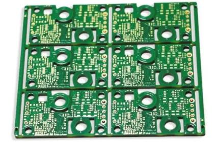
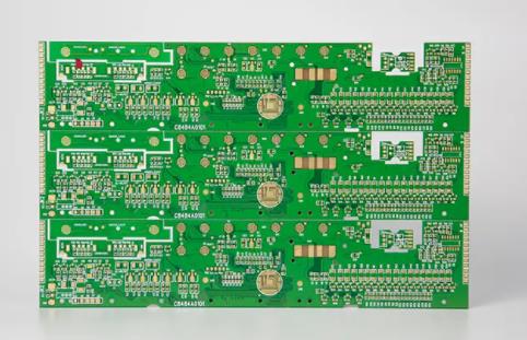
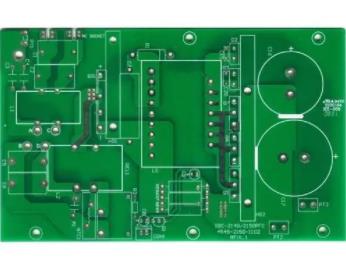
PCB制造
There are always several impedance discontinuities in PCB design
PCB manufacturers, PCB designers and PCBA manufacturers explain that there are always several impedance discontinuities in PCB design
characteristic impedance: also known as "characteristIC impedance", it is not DC resistance, but belongs to the concept of long line transmission. In the high-frequency range, during signal transmission, a transient current will be generated between the signal line and the reference plane (power supply or ground plane) along the place where the signal arrives due to the establishment of the electric field. If the transmission line is isotropic, there will always be a current I as long as the signal is transmitted. If the output voltage of the signal is V, the transmission line will be equivalent to a resistance in the process of signal transmission, the size of which is V/I. This equivalent resistance is calLED the characteristic impedance Z of the transmission line. In the process of signal transmission, if the characteristic impedance on the transmission path changes, the signal will reflect at the node with discontinuous impedance. The factors affecting the characteristic impedance include dielectric constant, dielectric thickness, line width and copper foil thickness.
1. Gradient line
Some RF devices are SMAll in package, and the SMD pad width may be as small as 12 mils, while the RF signal line width may be more than 50 mils. Gradual change lines shall be used and sudden change of line width is prohibited. The transition part of the gradient line should not be too long.
2. Corner
If the RF signal line is at right angles, the effective line width at the corner will increase and the impedance will be discontinuous, causing signal reflection. In order to reduce discontinuity, there are two methods to deal with corners: chamfer and fillet. The radius of the arc angle shall be large enough, generally speaking, R>3W.
3. Large pad
When there is a large pad on a 50 ohm thin microstrip line, the large pad is equivalent to a distributed capacitance, which destroys the continuity of the characteristic impedance of the microstrip line. Two methods can be taken at the same time to improve: first, thicken the microstrip line dielectric, and then, hollow the ground plane below the pad, both of which can reduce the distributed capacitance of the pad.
4. Through-hole
The through hole is a metal cylinder plated outside the through hole between the top layer and the bottom layer of the circuit board. Signal vias connect transmission lines on different layers. The residual pile through the hole is the unused part of the hole. Via pads are annular spacers that connect vias to the top or internal transfer lines. The isolation panel is an annular space in each power supply or ground plane to prevent short circuit to the power supply and ground plane. After strict physical theoretical derivation and approximate analysis, the equivalent circuit of the via can be modeled as a grounded capacitor connected in series at both ends of an inductor.
It can be seen from the equivalent circuit model that the vias themselves have parasitic capacitance to the ground. Suppose the reverse pad diameter of the vias is D2, the pad diameter of the vias is D1, the thickness of the PCB board is T, and the dielectric constant of the board substrate is ε, Then the parasitic capacitance of the via is approximate to:
The parasitic capacitance of the via can cause the signal rise time to be prolonged and the transmission speed to be slowed down, thus deteriorating the signal quality. SIMilarly, parasitic inductance also exists in vias. In high-speed digital PCBs, parasitic inductance often brings more harm than parasitic capacitance.
Its parasitic series inductance will weaken the contribution of bypass capacitor, thus weakening the filtering effectiveness of the whole power supply system. Assume that L is the inductance of the via, h is the length of the via, and d is the diameter of the central drilling hole. The approximate parasitic inductance of the via is:
a. The via is one of the important factors that cause the impedance discontinuity on the RF channel. If the signal frequency is greater than 1GHz, the effect of the via must be considered.
b. The common methods to reduce the impedance discontinuity of vias are: adopting diskless process, selecting outlet mode, optimizing the diameter of reverse pad, etc. Optimizing the diameter of the reverse pad is the most commonly used method to reduce the impedance discontinuity. Because the characteristics of vias are related to the structural dimensions such as aperture, pad, reverse pad, stack structure, and outlet mode, it is recommended that HFSS and Optimetrics should be used for optimization simulation according to the specific situation in each design.
c. When a parametric model is used, the modeling process is simple. During review, PCB designers are required to provide corresponding simulation documents.
d. The diameter of via, pad diameter, depth, and reverse pad will change, resulting in impedance discontinuity, reflection, and insertion loss.
5. Through hole coaxial connector
Similar to via structure, via coaxial connector also has impedance discontinuity, so the solution is the same as via. The common methods to reduce the impedance discontinuity of through-hole coaxial connector are the same: adopting diskless technology, appropriate outlet mode, and optimizing the reverse pad diameter. PCB manufacturers, PCB designers and PCBA manufacturers explain that PCB design always has several impedance discontinuities


抖音二維碼

Q Q二維碼

微信二維碼
點擊
然后
聯系
然后
聯系
電話熱線
13410863085Q Q

微信

- 郵箱