鑫景福致力于滿足“快速服務,零缺陷,輔助研發”PCBA訂購單需求。


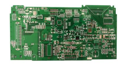
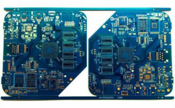
PCB制造
Influence of PCB Processing on Impedance Control and Its Solution
PCB manufacturers, PCB designers and PCBA manufacturers will explain the impact of PCB processing on impedance control and solutions
China is in the good situation of taking economIC construction as the center and reform and opening up. The annual growth rate of the electronic industry will exceed 20%. The printed circuit board industry, depending on the entire electronic industry, will also rise with the trend, and the growth rate will exceed 20%. The technological revolution and industrial structure changes in the world's electronic industry are bringing new opportunities and challenges to the development of printed circuits. With the development of miniaturization, digitalization, high frequency and multi-function of electronic equipment, printed circuit, as a metal wire in the electrical interconnection of electronic equipment, has become not only a problem of current flow, but also a function of signal transmission line. That is to say, for the electrical test of PCB used for transmission of high-frequency signal and high-speed digital signal, it is not only necessary to measure whether the circuit on-off and short circuit meet the requirements, but also to measure whether the characteristic impedance value is within the specified qualified range. Only when these two directions are qualified can the circuit board meet the requirements.
The circuit performance provided by the printed circuit board must be able to avoid reflection during signal transmission, and the signal can be kept intact to reduce transmission loss and play the role of matching impedance, so as to obtain a complete, reliable, accurate transmission signal without interference and noise. In this paper, the problem of characteristic impedance control of multilayers with surface microstrip line structure is discussed.
1. Surface microstrip line and characteristic impedance
The characteristic impedance value of the surface microstrip line is high and widely used in practice. Its outer layer is the signal line plane of the control impedance, which is separated from the adjacent datum plane by insulating materials. The calculation formula of the characteristic impedance is:
a. Microstrip
Z={87/[sqrt (Er+1.41)]} ln [5.98H/(0.8W+T)], where W is the line width, T is the copper sheet thickness of the wiring, H is the distance from the wiring to the reference plane, and Er is the dielectric constant of the PCB material. This formula can only be applied when 0.1<(W/H)<2.0 and 1<(Er)<15.
b. Stripline
Z=[60/sqrt (Er)] ln {4H/[0.67 π (0.8W+T)]} where H is the distance between two reference planes, and the routing is in the middle of the two reference planes. This formula can only be applied when W/H<0.35 and T/H<0.25
It can be seen from the formula that the main factors affecting the characteristic impedance are (1) the dielectric constant Er, (2) the dielectric thickness H, (3) the wire width W, and (4) the thickness T of the wire copper. Therefore, it can be seen that the characteristic impedance is closely related to the substrate material (copper clad plate), so the selection of the substrate material is very important in PCB design.
2. Dielectric constant of materials and its influence
The dielectric constant of the material is measured and determined by the manufacturer of the material at a frequency of 1Mhz. The same material produced by different manufacturers is different due to different resin content. This study takes epoxy glass cloth as an example to study the relationship between the dielectric constant and frequency change. The dielectric constant decreases with the increase of frequency. Therefore, in practical applications, the dielectric constant of the material should be determined according to the working frequency. Generally, the average value can meet the requirements. The transmission speed of the signal in the dielectric material will decrease with the increase of the dielectric constant. Therefore, to obtain a high signal transmission speed, the dielectric constant of the material must be reduced, At the same time, high characteristic resistance must be used to obtain high transmission speed, and low dielectric constant materials must be used for high characteristic resistance.
3. Influence of conductor width and thickness
The wire width is one of the main parameters that affect the change of characteristic impedance. Taking the surface microstrip line as an example, the figure illustrates the relationship between the impedance value and the wire width. It can be seen from the figure that when the wire width changes by 0.025mm, the corresponding impedance value will change by 5-6 ohms, while in actual production, if the signal line surface controlling the impedance uses 18 μ M Copper foil, the allowable variation tolerance of conductor width is ± 0.015mm, if the variation tolerance of control impedance is 35 μ M copper foil, the allowable variation tolerance of wire width is 0.025 mm. It can be seen that the allowable variation of wire width in production will lead to a great change in the impedance value. The wire width is determined by the designer according to a variety of design requirements. It should not only meet the requirements of wire current carrying capacity and temperature rise, but also obtain the desired impedance value. This requires that the producer should ensure that the line width meets the design requirements in production, and make it change within the tolerance range to meet the requirements of impedance. The conductor thickness is also determined according to the required current carrying capacity of the conductor and the allowable temperature rise. In order to meet the use requirements in production, the average coating thickness is generally 25 μ m. The thickness of the conductor is equal to the thickness of the copper foil plus the thickness of the coating. It should be noted that before electroplating, the conductor surface should be clean and free of residue and black plate oil, which may cause the copper not to be plated during electroplating, so that the local conductor thickness changes and affects the characteristic impedance value. In addition, be careful in the process of brushing the board, so as not to change the thickness of the wire and cause the impedance value to change.
4. Effect of medium thickness H
It can be seen from the formula that the characteristic impedance is proportional to the natural logarithm of the dielectric thickness. Therefore, the thicker the dielectric thickness is, the greater its impedance value is. Therefore, the dielectric thickness is another major factor affecting the characteristic resistance value. Because the wire width and the dielectric constant of the material have been determined before production, and the wire thickness process requirements can also be used as a fixed value, controlling the laminate thickness (dielectric thickness) is the main means to control the characteristic impedance in production. The relationship between the characteristic impedance value and the change of the dielectric thickness can be obtained. It can be seen that when the thickness of the medium changes by 0.025mm, the corresponding impedance value will change by+5-8 ohms, while in the actual production process, the allowable thickness change of each layer will cause a great change in the impedance value. In actual production, different types of prepreg are selected as the insulating medium, and the thickness of insulating medium is determined according to the number of prepreg. Take the surface microstrip line as an example: refer to Fig. in the production process. Determine the dielectric constant of the insulating material at the corresponding operating frequency, and then calculate the corresponding impedance value using the formula. Then, according to the wire width value and the calculated impedance value proposed by the user, find out the corresponding dielectric thickness through the diagram, and then determine the type and number of sEMI solidified sheets according to the thickness of the selected copper clad plate and copper foil.
5. Conclusion
In actual production, a slight change in the width and thickness of the conductor, the dielectric constant of the insulating material and the thickness of the insulating medium will cause a change in the characteristic impedance value. In addition, the characteristic impedance value is also related to other production factors. Therefore, in order to control the characteristic impedance, the manufacturer must understand the factors that affect the change of the characteristic impedance value, master the actual production conditions, and adjust each process parameter according to the requirements of the designer, Make it change within the allowable tolerance range to obtain the expected impedance value. PCB manufacturers, PCB designers and PCBA manufacturers explain the impact of PCB processing on impedance control and solutions


抖音二維碼

Q Q二維碼

微信二維碼
點擊
然后
聯系
然后
聯系
電話熱線
13410863085Q Q

微信

- 郵箱