鑫景福致力于滿足“快速服務,零缺陷,輔助研發”PCBA訂購單需求。


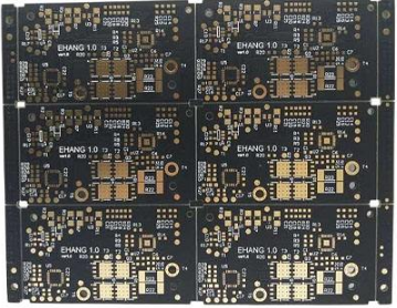
PCB制造
To design a printed circuit board (PCB) means to stop the circuit planning through the schematIC drawing and consume the PCB at the lowest possible cost. In the past, this was usually done with expensive special tools, but now, with the increasing improvement of high-performance software tools and design models, the design speed of PCB designers has been greatly accelerated.
Although the engineering designers know that a successful PCB design plan is the best way to prevent problems from appearing, it is still a way to waste time and money, while treating the root causes rather than the symptoms. For example, if problems are found in the electromagnetic compatibility (EMC) testing phase, a large amount of capital investment will be formed, so that the initial design plan will be adjusted and remanufactured, which will take months.
Planning is the first problem for PCB designers. This problem depends on the local content in the drawing, and some devices are set together based on logical thinking requirements. However, it should be noted that temperature sensitive components, such as sensors, should be set separately from heat generating components, including power converters. With regard to the design of PCB with multiple power settings, 12V and 15V power converters can be set at different positions of the circuit board, because the heat and electronic noise generated by them will affect the reliability and performance of other components and circuit boards.
The above PCB components will also affect the electromagnetic performance of the circuit design. This is not only important for the performance and energy consumption of the circuit board, but also for the economy of the circuit board. Therefore, all circuit board equipment sold in Europe must obtain the CE MARK to prove that it will not interfere with other systems. However, this is usually only from the perspective of power supply. There are also many devices that EMIt noise, such as DC-DC converters and high-speed data converters. Due to the defects of pcb design, these noises can be captured by the channel and stop radiating as a SMAll antenna, resulting in clutter noise and abnormal frequency areas.
The problem of far field electromagnetic interference (EMI) can be solved by installing filters at noise points or using metal enclosures to shield signals. However, adequate attention is paid to the equipment that can release electromagnetic interference (EMI) on the circuit board, which enables the circuit board to choose a lower price shell, thus effectively reducing the cost of the entire system.
In the PCB design process of the circuit board, electromagnetic interference (EMI) is indeed a factor that must be paid attention to. Electromagnetic crosstalk can couple with the channel, which disrupts the signal into noise and affects the overall performance of the circuit board. If the coupling noise is too high, the signal may be completely covered. Therefore, it is necessary to install an increasingly expensive signal amplifier in order to return to normal. However, if the signal circuit planning can be fully considered at the beginning of the circuit board design, the above problems can be prevented. Because the design of the circuit board will be different according to different equipment, different application locations, different heat dissipation requirements, and different electromagnetic interference (EMI) conditions, the design template will come into use.
Capacitance is also an important issue in circuit Board Design that cannot be ignored, because capacitance will affect the propagation speed of signals and increase the consumption of electricity. The channel will couple with the adjacent line or cross two circuit layers vertically, thus forming a capacitor unintentionally. By reducing the length of parallel lines and installing kinks on one of the lines to cut off the coupling, the above problems can be solved relatively easily. However, this also requires engineering designers to fully consider the criteria of consumption design, ensure that the design plan is convenient for manufacturing, and prevent any noise radiation caused by large bending angle of the line. The spacing between lines may also be too close, which will result in short circuits between lines, especially at line bends. As time goes on, metal "whiskers" will appear. Design rule detection can usually identify areas where the loop risk is higher than normal.
This problem is particularly prominent in the design of the ground plane. A metal circuit layer may form coupling with all lines above and below it. Although the metal layer can effectively block noise, it will also generate associated capacitance, which will affect the running speed of the line and increase the power consumption.
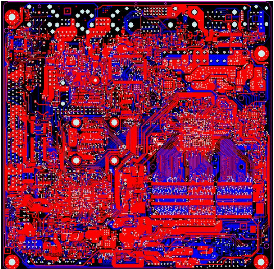
As far as the pcb design of multilayer circuit board is concerned, the through hole between different circuit board layers is probably the most controversial problem. The through-hole between the circuit board layers will affect the performance of the signal and reduce the reliability of the circuit board design, so it should be paid sufficient attention.
pcb design
Processing plan:
In the process of pcb design, many different methods can be adopted to deal with various problems. Among them, the adjustment of the existing design plan itself, such as adjusting the route planning to reduce noise; There are also ways to plan printed circuit boards. The design components can stop the automatic device through the planning tool. However, if the automatic planning can be manually adjusted, it will help to improve the quality of circuit board design. Through this measure, design rule detection will rely on PCB technical documents to ensure that the design of the circuit board can meet the requirements of the circuit board consumer manufacturers.
Separating different circuit board layers can reduce the associated capacitance. However, this will increase the number of layers of the circuit board, thus increasing the cost and bringing more through-hole problems. Although the use of orthogonal grid power supply system and grounding circuit design may increase the physical size of the circuit board, it can effectively play the role of the grounding layer in the double-layer circuit board, reducing the capacitance and the complexity of circuit board consumption and manufacturing.
Design tools, including DesignSpark PCB, can help engineering designers deal with many problems at the beginning of design, but engineering designers still need to have a full understanding of the design requirements of printed circuit boards (PCBs). For example, if the editor of a Printed Circuit Board (PCB) needs to have an understanding of the number of layers of the PCB at the beginning of the design, for example, a double-layer PCB needs to have a ground plane and a power plane, which are composed of two independent layers. The automatic component planning technology is very useful. It can help designers spend more time to design the planned area of equipment. For example, if the power supply equipment is too close to sensitive signal lines or areas with high temperature, many problems will arise. In the same way, signal lines can also stop automatic wiring and prevent most problems. However, stopping analysis and manual operation for high-risk areas will help greatly improve the quality of PCB design, improve benefits and reduce the overall cost.
Design rule detection is also a very powerful tool, which can stop the detection of lines to ensure that the spacing between lines is not too close, thus forming a short circuit. However, the overall pcb design still has high economic value. The design planning detection tool can also be used to detect and adjust the power layer and ground plane to prevent large associated capacitance area.


抖音二維碼

Q Q二維碼

微信二維碼
點擊
然后
聯系
然后
聯系
電話熱線
13410863085Q Q

微信

- 郵箱