鑫景福致力于滿足“快速服務,零缺陷,輔助研發”PCBA訂購單需求。


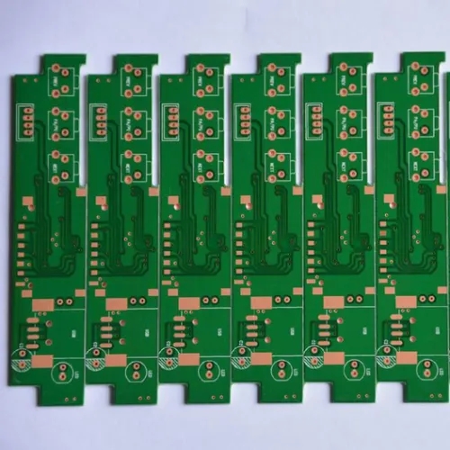
PCB制造
PCB design: noise reduction and electromagnetism, equal ability and responsibility
PCB manufacturers, PCB designers and PCBA manufacturers explain PCB design: noise reduction and electromagnetism, equal ability and responsibility
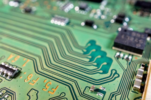
The sensitivity of electronIC equipment is getting higher and higher, which requires that the anti-interference ability of equipment is also getting stronger and stronger, so the design becoMES more difficult. How to improve the anti-interference ability of PCB has become one of the key issues that many engineers pay attention to, chip decryption. This paper will introduce some tips to reduce noise and electromagnetic interference in PCB design.
The following are 24 tips for reducing noise and electromagnetic interference in PCB design, which are summarized after years of chip decryption design:
(1) If you can use low-speed chips, you don't need high-speed chips. High speed chips are used in key places.
(2) The method of decrypting a resistor by a series of chips can reduce the jump rate of the upper and lower edges of the control circuit.
(3) Try to provide some form of damping for relays, etc.
(4) Use the clock with the lowest frequency meeting the system requirements.
(5) The clock generator tries its best to decrypt devices that are close to the clock. The shell of quartz crystal oscillator shall be grounded.
(6) Circle the clock area with a ground wire and keep the clock wire as short as possible.
(7) The I/O drive circuit shall be close to the edge of the printed board as far as possible, so that it can leave the printed board as soon as possible. The signal entering the PCB shall be filtered, and the signal from the high noise area
It is also necessary to add filtering. The chip is decrypted at the same time by means of serial terminal resistance to reduce signal reflection.
(8) The useless end of MCD shall be connected high, or grounded, or defined as an output end. The power supply and ground terminals on the integrated circuit shall be connected, and shall not be suspended.
(9) The unused gate circuit input terminal shall not be suspended, the unused op amp positive input terminal shall be grounded, and the negative input terminal shall be connected to the output terminal.
(10) As far as possible, PCB decryption uses 45 fold lines instead of 90 fold lines to reduce the external transmission and coupling of high-frequency signals.
(11) The printed circuit board shall be partitioned according to the frequency and current switching characteristics, and the noise components shall be further away from the non noise components.
(12) Single point power supply and single point grounding, power lines and ground wires shall be as thick as possible for single panel and double panel. If the economy is affordable, multi-layer boards shall be used to reduce power supply,
Decryption of the ground capacitance inductance chip.
(13) The clock, bus and chip selection signals shall be far away from I/O lines and connectors.
(14) Analog voltage input line and reference voltage terminal shall be far away from digital circuit signal line, especially clock.
(15) For A/D devices, the digital part and analog part of chip decryption should be unified rather than crossed.
(16) The clock line perpendicular to the I/O line has less interference than the parallel I/O line, and the clock element pin is far away from the I/O cable.
(17) The element pin shall be as short as possible, and the decoupling capacitor pin shall be as short as possible.
(18) The key lines shall be decrypted as thick as possible and protected on both sides. High speed lines should be short and straight.
(19) The lines sensitive to noise shall not be parallel to the high current and high-speed switching lines.
(20) Do not run wires under quartz crystal or noise sensitive devices.
(21) Do not form current loop around weak signal circuit and low-frequency circuit.
(22) The signal shall not form a loop. If it is unavoidable, the loop area shall be as SMAll as possible.
(23) Each integrated circuit has a decoupling capacitor. A small high-frequency bypass capacitor shall be added beside each electrolytic capacitor.
(24) Large capacity tantalum capacitors or Juku capacitors are used for chip decryption instead of electrolytic capacitors as circuit charging and discharging energy storage capacitors. When using tubular capacitors, the enclosure should be grounded.
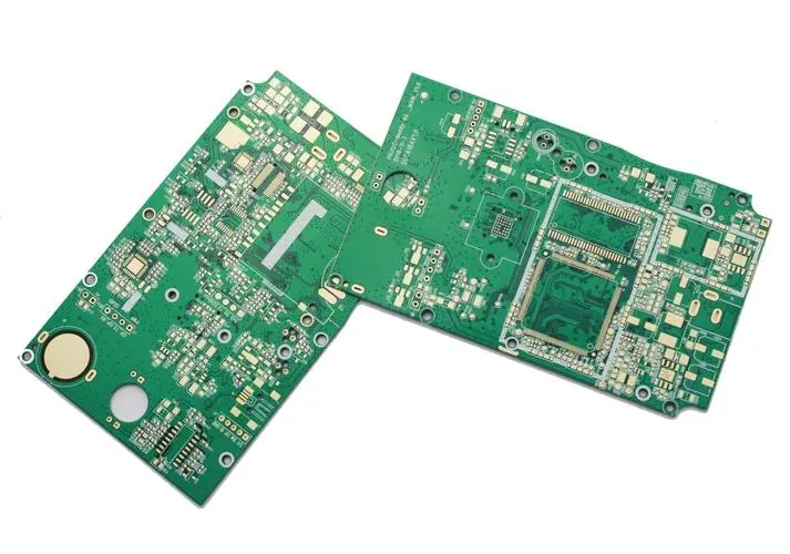
PCB copy: the greater the ability, the greater the responsibility
There is no doubt that the PCB industry is the largest part of the current electronic component industry, with an output value of 40 billion dollars. At the same time, as there is no mature technology and product that can replace PCB copying, its position in the electronic basic industry is unique and unshakable. In addition, although the area of PCB in a single final product is gradually decreasing, due to the improvement of precision and complexity, the value of PCB in the overall cost is increased because of the improvement of precision and complexity, It has become a pillar branch of the electronic component industry. Moreover, with the continuous expansion of PCB application field, the MARKet share in the future will further increase.
The market value and prOSPects of PCB copying enterprises are immeasurable. Accordingly, competition among peers is unavoidable. At present, enterprises within the industry can be roughly divided into three levels: high, middle and low. At that time, the middle and high end were dominated by foreign capital, Hong Kong and Taiwan capital, and a few state-owned enterprises. The low end refers to those small factories that lack equipment, capital, technology, and operation. The enterprise with the highest concentration is the mid tier enterprise, which is caught between two sides. From the current industry concentration, it is undeniable that there is fierce competition in the PCB copying industry, but it can also be seen that there is still a lack of large-scale large enterprises in the PCB copying industry.
PCB copying permeates every aspect of modern people's life. No matter communication, medical, aviation or transportation, it is inseparable from PCB. Therefore, the innovation of PCB copying industry is not only the reform within the industry, but also related to the reform of all aspects of social life. That is, the greater the ability, the greater the responsibility. PCB manufacturers, PCB designers and PCBA manufacturers explain PCB design: noise reduction and electromagnetism, equal ability and responsibility.


抖音二維碼

Q Q二維碼

微信二維碼
點擊
然后
聯系
然后
聯系
電話熱線
13410863085Q Q

微信

- 郵箱