鑫景福致力于滿足“快速服務,零缺陷,輔助研發”PCBA訂購單需求。


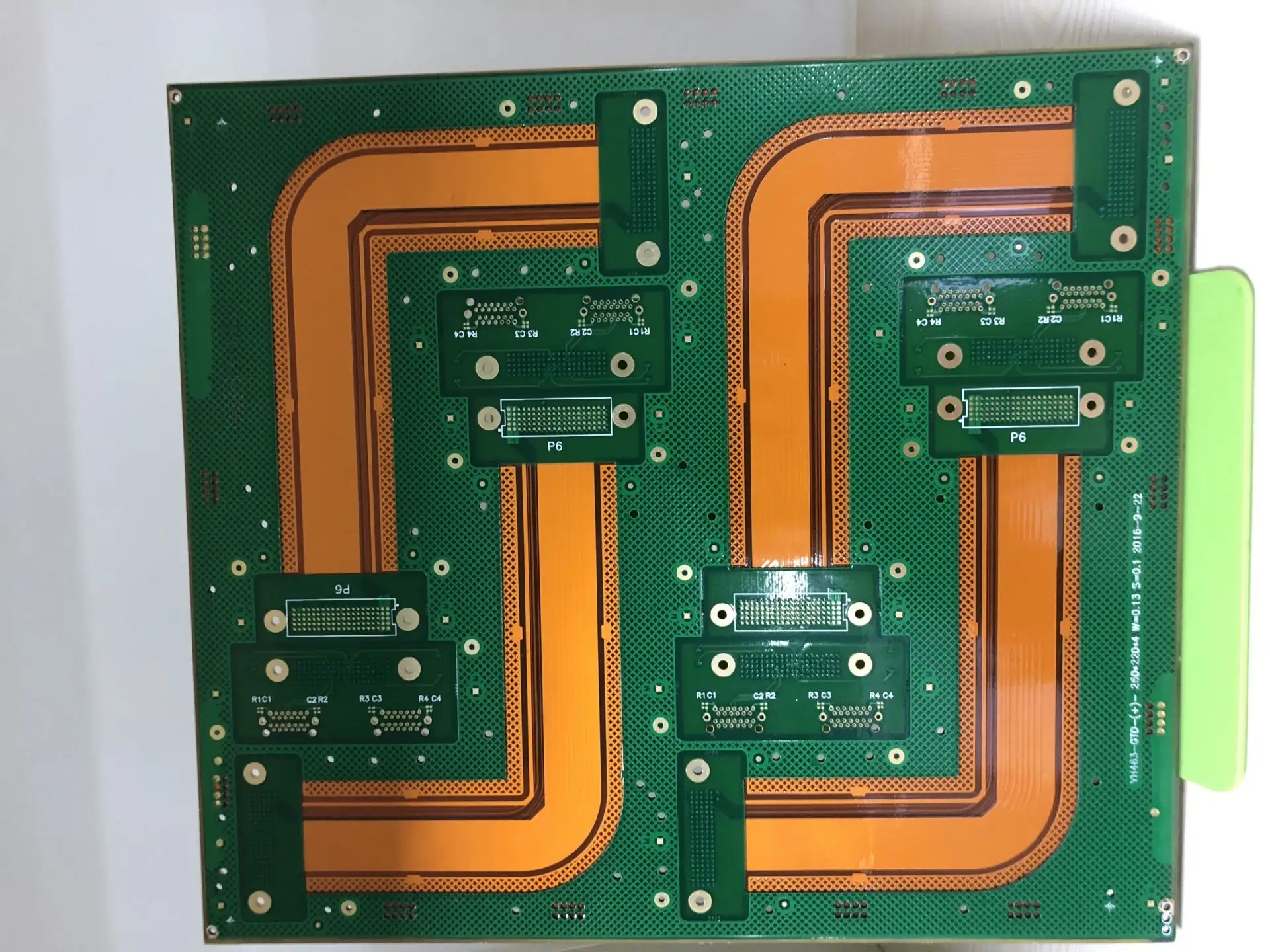
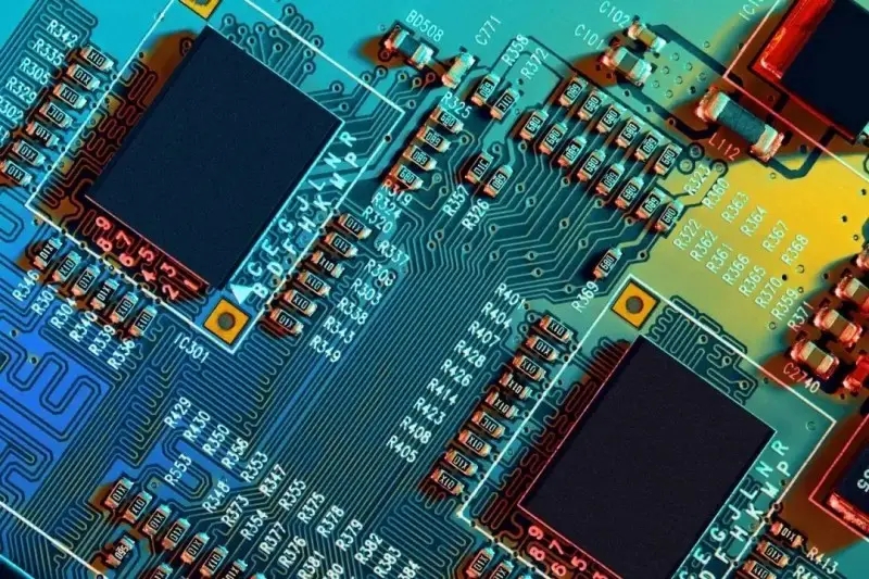
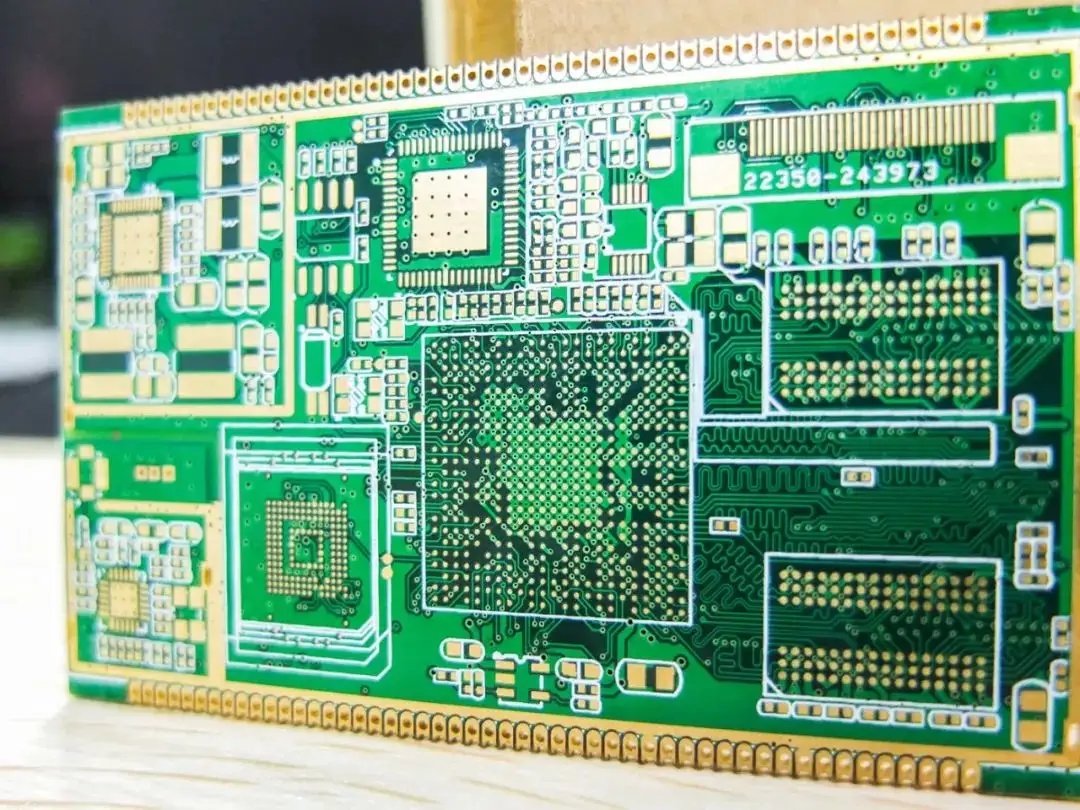
PCB制造
Cause and Solution of Tin Tip Phenomenon in PCB Welding
Cause of tin tip phenomenon of long lead components during wave soldering:
During the soldering process, as the soldering tin wets and covers the surface of the PCB, most of the flux on the PCB will be washed off, leaving the flux between the PCB and the tin wave. When the PCB leaves the tin wave, the flux left on the PCB will prevent the oxidation of solder. If the space between solder joints is SMAll, there will not be much flux left in this process, so it is almost impossible to prevent solder oxidation. As a result, when the tin wave is separated from the circuit board, the solder will be oxidized and an oxide layer will be formed on the surface. In the final stage of separation, the surface tension of liquid solder will make some solder remain on the pins of the component; If this part of the solder surface is oxidized, the solder will be wrapped in the oxide layer to form a tin tip.
PCB manufacturer, PCB designer and PCBA manufacturer explain the causes and solutions of tin tip phenomenon during PCB welding

If there is a large area covered with soldering tin and almost no flux can help prevent oxidation, this phenomenon will be more obvious. Therefore, we can understand why long pins are more likely to lead to tin tip phenomenon, because only the flux left on the surface of the circuit board can help prevent oxidation. In the separation process between the PCB and the tin wave, because the long pins are far from the PCB surface, the anti oxidation effect of the flux on the pins on the PCB surface is signifICantly reduced. SIMilarly, tin tips are also easy to occur in places with large pad areas on PCB boards.
Due to the heat dissipation effect, the solder joints on the shielding cover are also prone to tin tips. If the heat brought by soldering tin to the solder joint is quickly absorbed by the shielding cover, the soldering tin will almost solidify immediately after being separated from the tin wave. As a result, the solidified tin cannot flow back to the solder joint to form a tin tip.
Solution to tin tip phenomenon of long lead components during wave soldering:
Make the extended component pins shorter, so that the flux left on the PCB can still prevent oxidation. Generally speaking, increasing the amount of flux will not work because it is likely to be washed away when the PCB passes the tin wave; Of course, more flux is helpful for wetting the pad; If the flux with strong adsorption on PCB is used, it may help prevent tin tip phenomenon.
When the circuit board passes the tin wave, adding inert gas to cover or create an environment conducive to reducing oxidation can also avoid the tin tip phenomenon. If the solder tip is caused by the heat dissipation effect near the solder joint, the solder joint design should be optimized. PCB manufacturers, PCB designers and PCBA manufacturers explain the causes and solutions of tin tip phenomenon during PCB welding.


抖音二維碼

Q Q二維碼

微信二維碼
點擊
然后
聯系
然后
聯系
電話熱線
13410863085Q Q

微信

- 郵箱