鑫景福致力于滿足“快速服務,零缺陷,輔助研發(fā)”PCBA訂購單需求。


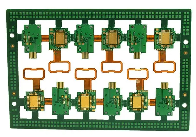
PCB制造
How to Clean the Bad Phenomenon in PCB and Customization
Circuit board manufacturers, circuit board designers and PCBA manufacturers explain how to clean the bad phenomena in circuit boards and customization
For a circuit board, reasonable cleaning can effectively ensure its good performance. What preparations should be made before cleaning? Let's get to know the PCB factory together.
Preparation before cleaning Before cleaning, all connectors on the circuit board, including jumper plugs, card boards, batteries and ICs, must be carefully pulLED out one by one. Potentiometers, transformers and solenoid coils (inductive coils) must also be removed from the circuit board. Therefore, once water enters the circuit board, the water droplets in the gap or between wire turns are difficult to be blown out by the compressed air and the moisture is difficult to be dried. Records must be made one by one during disassembly, To ensure that no error will occur during recovery after cleaning. At the same time, check whether the electrolytic capacitor on the circuit board has liquid leakage or bulge on the top. If yes, remove it and make a record so as to replace it with new products of equivalent value after the liquidation of the circuit board. For the circuit board of computer power supply, check whether there are cracks or loose solders between the pad and component pins of its printed circuit, especially the high-power components. If cracks or loose solders are found, repair them immediately. If one is found, repair one, otherwise it is easy to miss.
Therefore, make preparations before cleaning the circuit board to avoid damage to the circuit board due to incorrect operation.
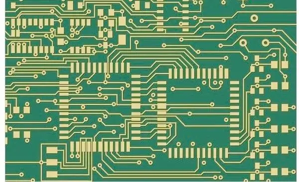
Bad phenomena in PCB customization
If the circuit board is poorly designed during the design process, it will affect the normal use. What are the common undesirable phenomena in the circuit board design? Let's talk to the Pcb factory.
The screw hole is used to fix the PCB board with screws. In order to prevent hole plugging after wave crest welding, copper foil is not allowed on the inner wall of the screw hole, and the screw hole pad on the wave crest surface needs to be designed as "meter" or quincunx.
2. The PCB is lack of process edge or the design of process edge is unfair, which causes the equipment cannot be mounted.
3. Common problems in pad size include pad size error, too large or too SMAll pad spacing, pad asymmetry, and unreasonable design of compatible pads.
4. The test point is too small, and the test point is placed below or too close to the element.
5. During welding, the solder melts and flows to the bottom of PCB, resulting in the defect of less tin in solder joints.
6. IC pad design is not standardized.
Therefore, in the process of PCB design, these problems should be solved in time to ensure its good performance. PCB manufacturers, PCB designers, and PCBA manufacturers will explain how to clean PCB and the undesirable phenomena in customization.


抖音二維碼

Q Q二維碼

微信二維碼
點擊
然后
聯(lián)系
然后
聯(lián)系
電話熱線
13410863085Q Q

微信

- 郵箱