鑫景福致力于滿足“快速服務,零缺陷,輔助研發”PCBA訂購單需求。


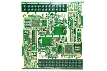
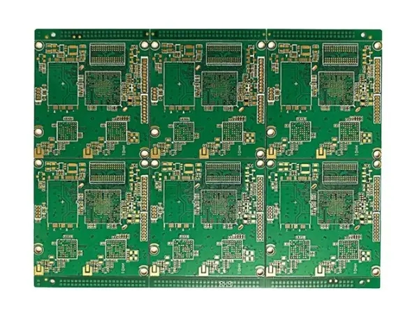
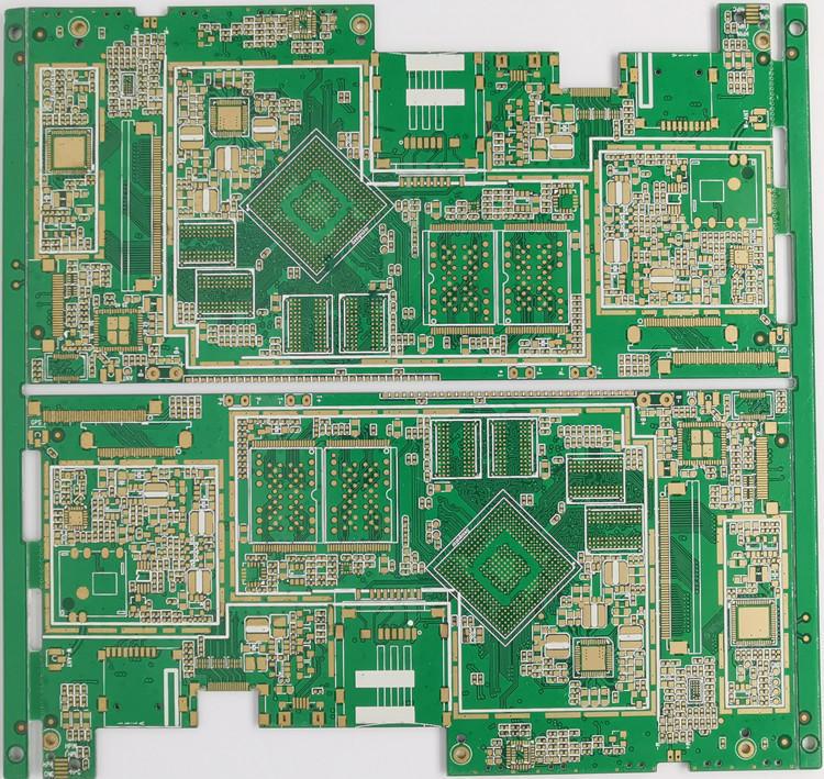
PCB制造
Summary and explanation of PCB surface treatment steps
PCB manufacturing, PCB design and PCBA processing manufacturers will explain the PCB surface treatment steps to you
The basIC purpose of PCB surface treatment Z is to ensure good solderability or electrical properties. As the copper in nature tends to exist in the form of oxide in the air, it is unlikely to remain the original copper for a long time, so other treatment is required for copper
1. Hot air leveling (tin spraying)
Hot air leveling, also known as hot air solder leveling (commonly known as tin spraying), is a process of coating molten tin (lead) solder on the PCB surface and leveling (blowing) it with heated compressed air to form a coating that is both resistant to copper oxidation and can provide good solderability. Copper tin intermetallic compound is formed at the joint of solder and copper during hot air leveling. PCB shall be immersed in molten solder during hot air leveling; The air knife blows the liquid solder before the solder solidifies; The wind knife can reduce the meniscus Z of solder on the copper surface and prevent solder bridging.
2. Organic Solderability Protector (OSP)
OSP is a process for copper foil surface treatment of printed circuit boards (PCBs) that meets the requirements of RoHS instructions. OSP is the abbreviation of Organic Solderability Preservatives, which is translated into organic solder mask, also known as copper protector, or Preflux in English. To put it SIMply, OSP is to chEMIcally grow an organic film on the clean bare copper surface. This film has oxidation resistance, heat shock resistance and moisture resistance to protect the copper surface from further rusting (oxidation or vulcanization, etc.) in normal environment; However, in the subsequent high welding temperature, this protective film must be easily removed by the flux, so that the exposed clean copper surface can be immediately combined with the molten solder in a very short time to become a solid solder joint.
3. Full plate nickel plated gold
Nickel gold plating on the PCB surface refers to coating the conductor with a layer of nickel first and then a layer of gold. Nickel plating is mainly used to prevent the diffusion between gold and copper. Now there are two types of nickel gold plating: soft gold plating (pure gold, the gold surface looks not bright) and hard gold plating (the surface is smooth and hard, wear-resistant, containing cobalt and other elements, the gold surface looks bright). Soft gold is mainly used to make gold wire during chip packaging; Hard metal is mainly used for electrical interconnection at non welding points.
4. Sinking gold
Gold deposition is to wrap a thick layer of nickel gold alloy with good electrical properties on the copper surface, which can protect PCB for a long time; In addition, it also has the environmental tolerance that other surface treatment processes do not have. In addition, gold deposition can also prevent the dissolution of copper, which will be beneficial to lead-free assembly.
5. Tin precipitation
At present, all solders are based on tin, so the tin layer can match any type of solder. The tin deposition process can form a flat copper tin intermetallic compound, which makes the tin deposition have the same good solderability as the hot air leveling without the headache flatness problem of the hot air leveling; The tin plate cannot be stored for too long, and the assembly must be carried out according to the sequence of tin deposition.
6. Sink silver
Silver deposition process is between organic coating and electroless nickel/gold plating, which is relatively simple and fast; Even if exposed to heat, humidity and pollution, silver can still maintain good solderability, but it will lose luster. Silver deposition does not have the good physical strength of electroless nickel/gold plating because there is no nickel under the silver layer.
7. Chemical nickel palladium
Compared with gold precipitation, chemical nickel palladium has an additional layer of palladium between nickel and gold. Palladium can prevent corrosion caused by displacement reaction and make full preparation for gold precipitation. Gold tightly covers palladium, providing a good contact surface.
8. Hard gold electroplating
In order to improve the wear resistance of the product and increase the number of plug and pull, hard gold is plated. PCB manufacturing, PCB design and PCBA processing manufacturers will explain PCB surface treatment steps to you.


抖音二維碼

Q Q二維碼

微信二維碼
點擊
然后
聯系
然后
聯系
電話熱線
13410863085Q Q

微信

- 郵箱