鑫景福致力于滿足“快速服務(wù),零缺陷,輔助研發(fā)”PCBA訂購單需求。


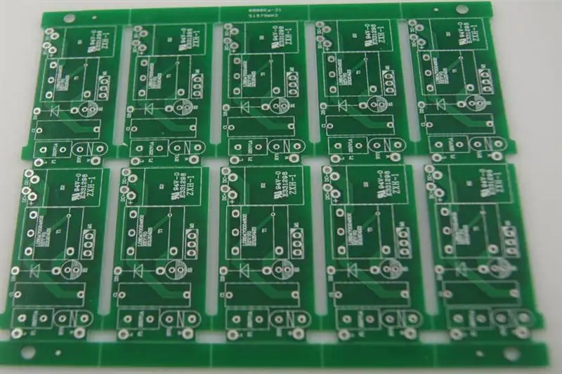
PCB制造
Etching Quality and Early Problems of HF Board Outer Circuit
The Circuit board manufacturer, circuit board designer and PCBA processor will explain the etching quality of the outer circuit of the high-frequency board and the previous problems
Etching quality and previous problems
The basIC requirement for etching quality is to completely remove all copper layers except under the corrosion resistant layer. Strictly speaking, if we want to define accurately, the etching quality must include the consistency of wire width and the degree of side etching. Due to the inherent characteristics of the current corrosion solution, it not only etches downward, but also etches left and right, so side erosion is almost inevitable.
Side etching is a frequently discussed item in etching parameters. It is defined as the ratio of side etching width to etching depth, which is calLED etching factor. In the printed circuit industry, it has a wide range of changes, from 1:1 to 1:5. Obviously, SMAll side etching degree or low etching factor is the most satisfactory.
The structure of the etching equipment and the etching solution with different components will have an impact on the etching factor or side etching degree, or in optimistic terms, it can be controlled. The side erosion can be reduced by using some additives. The chEMIcal composition of these additives is generally a trade secret, and their respective developers do not disclose it to the outside world. As for the structure of etching equipment, the following chapters will be devoted to the discussion.
In many ways, the quality of etching has existed long before the PCB entered the etching machine. Because there is a very close internal relationship between each process or process of processing printed circuit (PCB high-frequency board/Logers high-frequency hybrid board), there is no process that is not affected by other processes and does not affect other processes. Many problems identified as etching quality have actually existed in the process of film removal or even earlier. As for the etching process of the outer graphic, because the "inverted stream" that it represents is more prominent than most PCB processes, many problems are finally reflected in it. At the same time, this is also because etching is the last step in a long series of processes starting from film pasting and photosensitivity. After that, the outer pattern is successfully transferred. The more links, the greater the possibility of problems. This can be seen as a very special aspect of the printed circuit production process.
Theoretically, after the printed circuit enters the etching stage, in the process of processing printed circuit by pattern electroplating, the ideal state should be: the total thickness of copper and tin or copper and lead tin after electroplating should not exceed the thickness of the electroplating sensitive film, so that the electroplating pattern is completely blocked by the "wall" on both sides of the film and embedded in it. However, in real production, after electroplating, the coating pattern of printed circuit boards all over the world should be much thicker than the photosensitive pattern. In the process of electroplating copper and lead tin, because the coating height exceeds the photographic film, there will be a trend of horizontal accumulation, which leads to the problem. The tin or lead tin anti-corrosive layer covered above the strip extends to both sides to form an "edge", covering a small part of the photosensitive film under the "edge".
The "edge" formed by tin or lead tin makes it impossible to completely remove the photosensitive film when removing the film, leaving a small part of "glue residue" below the "edge". "Residual glue" or "residual film" left below the "edge" of the resist will cause incomplete etching. "Copper root" is formed on both sides of the line after etching. The copper root narrows the line spacing, causing the printed board to fail to meet the requirements of Party A, and may even be rejected. Rejection will greatly increase the production cost of PCB high-frequency board/Logers high-frequency hybrid board.
In addition, in many cases, the dissolution is formed due to the reaction. In the printed circuit industry, the residual film and copper may also form a pile up in the corrosion solution and be blocked in the nozzle of the corrosion machine and the acid resistant pump, which has to be shut down for treatment and cleaning, thus affecting the working efficiency. circuit board manufacturers, circuit board designers and PCBA processors will explain the etching quality of the outer circuit of high-frequency boards and the existing problems.


抖音二維碼

Q Q二維碼

微信二維碼
點擊
然后
聯(lián)系
然后
聯(lián)系
電話熱線
13410863085Q Q

微信

- 郵箱