鑫景福致力于滿足“快速服務,零缺陷,輔助研發”PCBA訂購單需求。


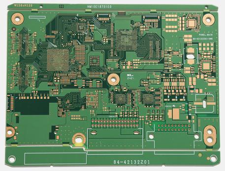
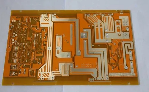
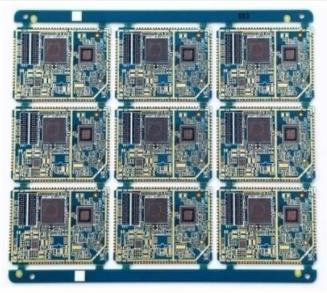
PCB制造
Different warpage degrees of PCB factory boards? ThICkness of PCB electroplating film
PCB manufacturers, PCB designers and PCBA manufacturers explain to you why the warpage of PCB boards is different? Thickness of PCB electroplating film
Why does the warpage of Pcb factory boards differ? Come and have a look with Xiao Bian
1. Uneven copper surface area on the circuit board will worsen PCB warpage.
Generally, PCB manufacturers will design a large area of copper foil on the circuit board for grounding. SometiMES, the Vcc layer will also be designed with a large area of copper foil. When these large areas of copper foil cannot be evenly distributed on the same circuit board, it will cause the problem of uneven heat absorption and heat dissipation. Of course, the circuit board will also expand with heat and contract with cold. If the expansion and contraction cannot occur at the same time, it will cause different stresses and deformation, At this time, if the temperature of the board has reached the upper limit of Tg value, the board will begin to soften, causing permanent deformation.
2. The vias on each layer of the circuit board will limit the expansion and contraction of the board
Nowadays, most circuit boards in PCB factories are multilayer boards, and there will be vias like rivets between layers. The vias are divided into through holes, blind holes and embedded holes. Where there are vias, the effect of cold expansion and contraction of boards will be limited, and PCB warping will be indirectly caused.
3. The weight of the circuit board itself will cause warping and deformation of the board
Generally, the reflow soldering furnace uses a chain to drive the circuit board forward, that is, the two sides of the board are used as fulcrums to support the whole board. If there are overweight parts on the board or the size of the board is too large, the board will show a hollow in the middle due to its own weight, causing warping.
4. The depth of V-Cut and the connecting strip will affect the deformation of the panel
Basically, V-Cut is the culprit of destroying the board substructure. Because V-Cut cuts V-shaped grooves on the original large sheet, the V-Cut area is prone to deformation.
The thickness of electroplated film on automobile circuit board varies from day to day? Why is it thin and thick?
During the processing of automobile circuit board patch, an electroplated film may appear, but if the thickness of the electroplated film does not exceed the standard thickness, it will not affect the use of automobile circuit board, but if it is too thin and thick, it may affect the welding and subsequent use of automobile circuit board patch. Today, let's roughly understand the reason why the electroplated film is too thick and thin.
The essence of electroplating process is the process in which metal ions are reduced to metal crystals to form a coating. Therefore, the factors that affect the coating thickness are also factors that affect the electrocrystallization process. From the electrochEMIcal point of view, Faraday's law and electrode potential equation can be used as the basis for analyzing the factors affecting the coating thickness;
According to Faraday's Law, the amount of metal ions reduced to metal at the electrode is proportional to the amount of electricity. Therefore, the current is an important factor affecting the thickness of the coating. Specifically, in the electroplating process, it is the effect of current density. High current density leads to high deposition speed of the coating;
Of course, electroplating time is also an important factor to determine the coating thickness. Obviously, in general, time and current density are proportional to the coating thickness;
In addition to the current density and time, temperature, main salt concentration, anode area, bath stirring, etc. will have an impact on the thickness of the coating. However, analysis shows that temperature, main salt concentration, anode area, bath stirring all affect the thickness of the coating by affecting the current density;
At high temperature, the current density can be increased. SIMilarly, stirring the bath can also increase the current density, which is conducive to increasing the coating thickness. Maintaining the anode area is very important for maintaining normal current distribution and normal dissolution of the anode, which has a direct impact on the coating thickness. Only when the main salt concentration is within the normal range, can electroplating be allowed to work within the normal current density range.
These are the reasons why the electroplating film is too thick and thin. You can refer to them when designing and processing automobile circuit board patches at ordinary times to avoid some unnecessary losses. PCB manufacturers, PCB designers and PCBA manufacturers explain to you why the warpage of PCB boards is different? The thickness of pcb electroplating film.


抖音二維碼

Q Q二維碼

微信二維碼
點擊
然后
聯系
然后
聯系
電話熱線
13410863085Q Q

微信

- 郵箱