鑫景福致力于滿足“快速服務(wù),零缺陷,輔助研發(fā)”P(pán)CBA訂購(gòu)單需求。


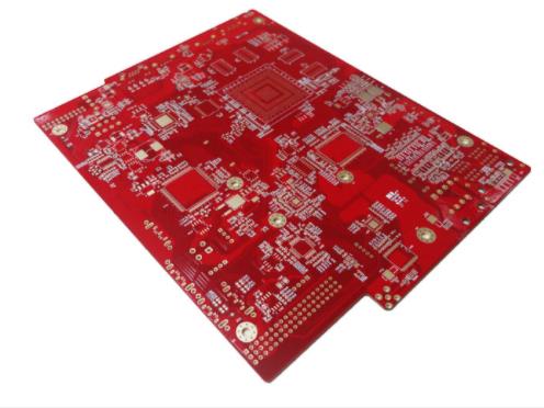
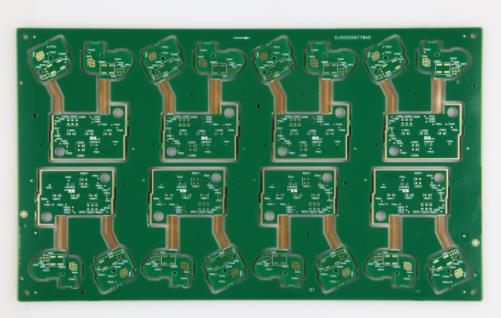
PCB制造
The circuit board manufacturer explained what problems would occur during HDI punching?
PCB manufacturers, PCB designers and PCBA manufacturers explain to you what problems will occur when PCB manufacturers explain HDI punching process?
HDI is the abbreviation of High Density Interconnector. High Density Interconnection (HDI) manufacturing is the fastest growing field in the printed circuit board industry. From the first 32-bit computer launched by HP in 1985 to the large client server that now uses 36 sequential laminated multilayer printed boards and stacked mICro vias, HDI/micro vias technology is undoubtedly the future PCB architecture. Large ASICs and FPGAs with SMAller device spacing and more I/O pins and embedded passive devices have shorter rise tiMES and higher frequencies. They all require smaller PCB Feature sizes, which drives a strong demand for HDI/micro vias.
Punching is an important process in HDI PCB proofing. What problems will occur during HDI punching? Now let's get to know with HDI factory.
1、 Rough section
1. Cause:
(1) The blanking clearance of concave and convex dies is too large; The cutting edge of the female die is seriously worn.
(2) The blanking force of the punch is insufficient and unstable.
(3) The blanking performance of sheet metal is poor.
2. Solution:
(1) Select the appropriate blanking clearance of concave and convex dies.
(2) Timely trim the cutting edge of the female die.
(3) Select the base material with good blanking performance and control the preheating temperature and time strictly according to the process requirements.
2、 Hole of hole and crack between holes
1. Cause:
(1) The hole wall is too thin, and the radial extrusion force during punching exceeds the hole wall strength of the plate.
(2) The two adjacent holes are not punched out at the same time, and the back punched holes are cracked due to the thin hole wall.
2. Solution:
(1) The hole spacing shall be designed reasonably, and the hole wall shall not be less than the thickness of the base plate.
(2) The adjacent holes shall be punched out SIMultaneously with a pair of moulds.
3、 External bulging
1. Cause:
The mold design is unreasonable; The concave die of profile blanking is deformed, and the long side is bulging.
2. Solution:
(1) When the overall dimension of the printed board is greater than 200 mm, it is advisable to adopt the die shape of the feeding and blanking structure.
(2) Increase the wall thickness of the female die, or select materials with sufficient bending and tensile strength to make the die.
4、 Scrap jumping up
1. Cause:
(1) The adhesion between the copper foil and the base material is poor, and the copper foil on the scrap is easy to fall off when punching. When the punch exits the female die, it enters the punched hole.
(2) The clearance of the die is too large and the leakage is not smooth. When the punch exits the die for discharging, the waste will jump up.
(3) The die hole has an inverted cone, and the punching waste is difficult to fall, but it jumps up as the punch exits the die.
2. Solution:
(1) Strengthen the incoming inspection of substrate materials.
(2) Reduce the clearance between concave and convex dies, and expand the leakage hole.
(3) Trim the inverted cone of the die hole in time.
5、 Waste clogging
1. Cause:
(1) The cutting edge of the die is too high and there is too much waste.
(2) The concentricity of the leakage hole on the lower base plate and the lower die seat is different from that of the die hole, and the hole butt joint is like a step.
(3) The leakage hole is too large, and the waste is easy to be stacked irregularly in the hole; The adjacent two leakage holes are also easy to be blocked when they are cut in.
2. Solution:
(1) Reduce the cutting edge of the female die, and the number of waste materials can be reduced between 0.2 mm.
(2) Adjust the vertical concentricity of the material leakage hole on the female die, lower backing plate and lower die base, and
Hole enlargement.
(3) When two adjacent leakage holes are cut internally, they shall be made into a round waist hole or a large hole in order not to block the leakage. PCB manufacturers, PCB designers and PCBA manufacturers explain to you what problems will occur when PCB manufacturers explain HDI punching process?


抖音二維碼

Q Q二維碼

微信二維碼
點(diǎn)擊
然后
聯(lián)系
然后
聯(lián)系
電話熱線
13410863085Q Q

微信

- 郵箱