鑫景福致力于滿足“快速服務,零缺陷,輔助研發”PCBA訂購單需求。


PCB制造
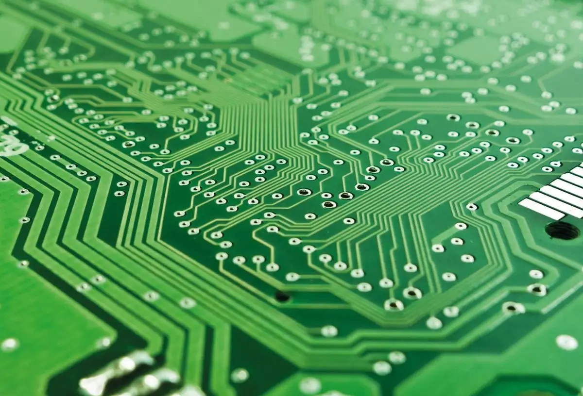
Open almost any electronIC product and inside is a Printed Circuit Board (PCB). The board provides the mechanical mounting for the electronIC components that make up the design and the electrical connections between them. Commonly used in the electronics industry for more than half a century, PCBs have evolved into complex objects created by skilLED designers and fabricated using precision craftSMAnship.
While understanding how PCBs are manufactured is not mandatory for designers, those who master the process are better able to design lower cost PCBs and thus benefit from higher manufacturing yields.
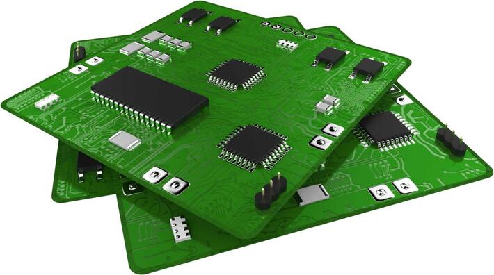
assembled printed circuit board stack
PCB (printed circuit board) is the heart of almost all electronic products.
Anatomy of a PCB
The following sections describe the various types of PCBs - from single-sided to rigid-flex - and factors common to all manufacturing processes.
single panel
The easiest PCB to make is called a single-sided PCB because it has conductors on only one side; usually the bottom.
Single-sided PCB with space for components on the top and space for soldering on the bottom.

A single-sided PCB has roughly the same lifespan as all PCBs, i.e. as an insulating substrate called a core. The core can be made of a variety of materials, depending on the properties required for the final circuit, but the most common material is fiberglass.
The insulating core is usually manufactured using a material called FR4. This is a flame retardant, Type 4 woven glass reinforced epoxy laminate - a strong rigid insulator that retains its high mechanical and electrical insulating properties in both dry and wet conditions and also has good manufacturing properties.
One side of the core is completely coated with a thin layer of copper. The drilled holes will be used to mount the components, using a chEMIcal etching process to remove unwanted copper, leaving the tracks and pads needed to electrically connect the circuit components together.
The top of the board is called the component side, because through-hole components are usually mounted on this side, so their leads protrude from the board to the bottom, where they can be more easily soldered to copper pads and tracks. surface mount components are an exception to this rule, as they need to be mounted directly to the copper pads and can only exist on the solder side.
Double panel
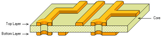
Only slightly more complex than single-sided PCBs are double-sided PCBs, which have copper traces on the top and bottom sides of the core. This allows for more complex routing. By convention, through-hole components are still mounted on the top layer, while surface mount components are still mounted on the bottom layer, according to a single-sided PCB.
Double Sided PCB, Unplated Through Hole, Cutaway View
Double-sided PCB with conductive tracks on the top and bottom of the board.
Plated Through Hole (PTH)

Double-sided panels typically rely on the leads of through-hole components to provide electrical connections between the top and bottom layers. However, this is not always possible as it is sometiMES necessary to traverse the traces between the two layers at locations that do not coincide with the component leads. Therefore, a common addition to double-sided PCBs is plated through holes (PTH).
Double Sided PCB, Plated Through Hole, Cutaway View
Double-sided PCB with plated through holes.
Hole plating is accomplished using an electrolytic process to deposit copper inside the hole after drilling. This creates a conductive path between the copper on the top and bottom layers, independent of the leads of through-hole components.
Top and bottom solder mask

Most PCB assemblies are soldered using a wave or reflow process. In either case, unless a solder mask is applied, solder bridging may occur between adjacent traces. As the name suggests, solder mask provides a repellant (or mask) that helps prevent solder from indiscriminately sticking to copper in areas of the circuit board that would otherwise lead to failure. As a secondary benefit, solder mask also prevents corrosion of exposed copper on PCB traces.
Double Sided PCB, Plated Through Holes and Solder Mask, Cutaway View
Double-sided PCB with plated through holes and solder mask.
While almost any color can be used, solder mask is traditionally green and is why most people think that PCBs have the characteristic green color. Soldermask is applied to the top and bottom layers of the PCB using a precision screen printing process.
Silk screen layer
When visible information such as a company logo, part number, or description needs to be applied to a board, silkscreen is used to apply text to the outer surface of the board. Silkscreen information is usually white to contrast with the solder mask of choice, but any color can be used. Where spacing permits, screened text can indicate component designators, switch setting requirements, and additional features to aid the assembly process.
Double-sided PCB, silk screen top view
Silkscreen information has been added to the top of the PCB to indicate the component designator.
So far, only PCBs with one or two copper layers have been described, but it is possible to create PCBs with more layers. These PCBs are called multi-layer PCBs, and they can provide denser routing topologies and better electrical noise characteristics. Each layer in a multilayer PCB is either a signal layer or a plane layer.
Signal Layers - These layers are entirely reserved for transmitting electrical signals from one component to another.
Planar Layers - These layers consist of bulk copper and are typically used for power supplies like VCC and GND. By utilizing a large surface area, planar layers are excellent at preventing and suppressing electrical noise.
Multilayer PCB, exploded 3D view
An exploded view of the PCB, including red, light green, and light brown signal layers, and green and dark brown plane layers.
multilayer PCBs can be manufactured in a few different ways, but the easiest is to laminate multiple thin double-sided PCBs together, using a layer of prepreg between each PCB.

Prepreg - short for preimpregnated - is a flexible material, often also containing woven glass, that is offered to PCB manufacturers to be partially cured (not fully cooked). It is contained between rigid layers in a layer stack during the manufacturing process and then heated for final curing, after which it becomes rigid, helping to connect the layers and form the overall structure of the finished board.


抖音二維碼

Q Q二維碼

微信二維碼
點擊
然后
聯系
然后
聯系
電話熱線
13410863085Q Q

微信

- 郵箱