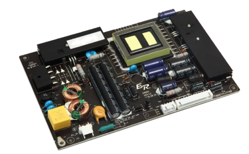
鑫景福致力于滿足“快速服務,零缺陷,輔助研發”PCBA訂購單需求。


PCB制造
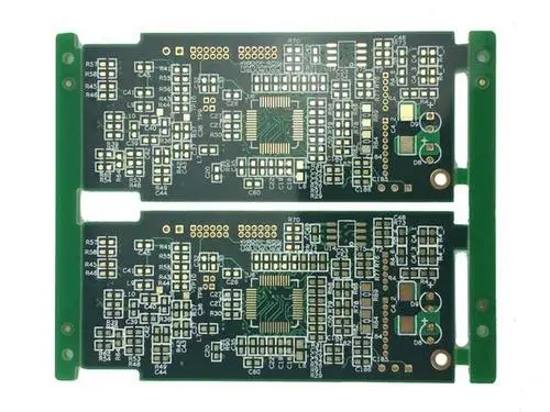
PCB circuit board is generally divided into six layers, specifICally: mechanical layer, prohibited wiring layer, solder mask layer, soldering aid layer, silk screen layer and via layer.
Mechanical layer
Protel 99 SE provides 16 mechanical layers, which are generally used to set the overall dimensions, data MARKs, alignment marks, assembly instructions and other mechanical information of the circuit board. The information varies according to the requirements of the design company or PCB manufacturer. Execute the menu command Design | MechanicalLayer to set more mechanical layers for the circuit board. In addition, the mechanical layer can be attached to other layers to output and display together.
Keep Out Layer
It is used to define the area where components and wiring can be effectively placed on the circuit board. Draw a closed area on this layer as the valid routing area. You cannot automatically layout and route outside this area.
Solder mask
Apply a layer of paint, such as solder mask, on all parts outside the bonding PCB pad to prevent tin coating on these parts. The solder mask is automatically generated for matching pads during the design process.
Welding flux
The soldering aid layer is used when the machine is mounting. It is the same size as the top layer/bottom layer and corresponds to the bonding pads of all mounting PCB components. It is used to open the tin leakage of the steel MESh.
Silkscreen
The silk screen layer is mainly used to place printed information, such as outline and annotation of components, various annotation characters, etc. Protel 99 SE provides two silk screen layers: Top Overlay and Bottom Overlay. Generally, all marking characters are on the top screen layer, and the bottom screen layer can be closed.
Borehole layer
The drilling layer provides the drilling information during the manufacturing process of the circuit board (such as the pad, through hole drilling is required). Protel 99 SE provides two drilling layers, namely, Drillgrid and Drill drawing.
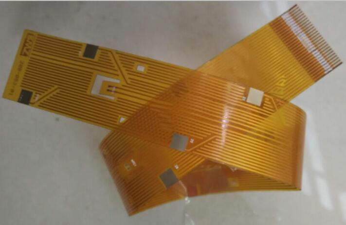
The main development direction of PCB now is also SMAll and precise. Only when the staff of Jieduobang take each PCB seriously, can they provide customers with more sophisticated PCB.


抖音二維碼

Q Q二維碼

微信二維碼
點擊
然后
聯系
然后
聯系
電話熱線
13410863085Q Q

微信

- 郵箱