鑫景福致力于滿足“快速服務,零缺陷,輔助研發”PCBA訂購單需求。


PCB制造
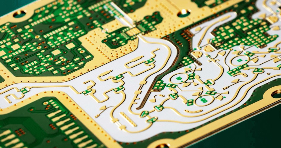
What are the differences between the layers of a PCB?
During PCB design, I found that many people do not know enough about the layers in PCB, especially novICes, who are vague about the role of each layer. So today, let's take a look at the differences between different layers when using the Altium designer palette.
1. Signal layer
The signal layer is divided into Top Layer and Bottom Layer, which are the layers with electrical connections. They can place components and wires.
2. Mechanical layer
Mechanical (mechanical layer) defines the appearance of the entire PCB. The reason why "mechanical" is emphasized is that it does not have electrical attributes. Therefore, it can be safely used to sketch shapes, sketch mechanical dimensions, place text, etc., without worrying about any changes to the electrical characteristics of the board. Up to 16 mechanical layers can be selected.
3. Silk screen layer
Top Overlay and Bottom Overlay are used to define the screen printed characters on the top and bottom layers, which are text symbols printed on the solder mask layer, such as component naMES, component symbols, component pins and copyrights, to facilitate future circuit welding and error checking.
4. Solder paste layer
The solder paste layer includes the top paste layer and the bottom paste layer. It refers to the exposed surface mounted pads that we can see, that is, the parts that need to be coated with solder paste before welding. Therefore, this layer is also useful for hot air leveling of pad and welding steel mesh fabrication.
5. Solder mask
Solder resistance layer is also often referred to as "window opening", including the top solder layer and bottom solder layer. Its function is opposite to that of solder paste layer, which refers to the layer to be covered with green oil. This layer does not stick solder to prevent short circuit of excess solder at adjacent welding points during welding. The solder mask covers the copper film conductor, preventing the copper film from oxidation in the air too quickly, but leaving a place at the solder joint, not covering the solder joint.
Conventional copper coating or wiring is covered with green oil by default. If we treat the solder barrier layer accordingly, it will prevent the green oil from covering and expose the copper.
6. Borehole layer
The drilling layer includes two drilling layers, namely, Drill Grid and Drill Drawing. The drilling layer is used to provide drilling information during the manufacturing process of the circuit board (such as pads, which need to be drilLED through holes).
7. No wiring layer
Keep Out Layer is used to define the boundary of the wiring layer. After defining the prohibited wiring layer, the wiring with electrical characteristics cannot exceed the boundary of the prohibited wiring layer in the subsequent wiring process.
8. Multilayer
Multi layer. The pads and through-hole on the circuit board need to penetrate the entire circuit board to establish electrical connections with different conductive graphic layers. Therefore, the system has set up an abstract layer - multilayer. Generally, pads and vias must be set on multiple layers. If this layer is closed, pads and vias cannot be displayed.

How to place pcb components
10-25,2022


抖音二維碼

Q Q二維碼

微信二維碼
點擊
然后
聯系
然后
聯系
電話熱線
13410863085Q Q

微信

- 郵箱