鑫景福致力于滿足“快速服務,零缺陷,輔助研發”PCBA訂購單需求。


PCB制造
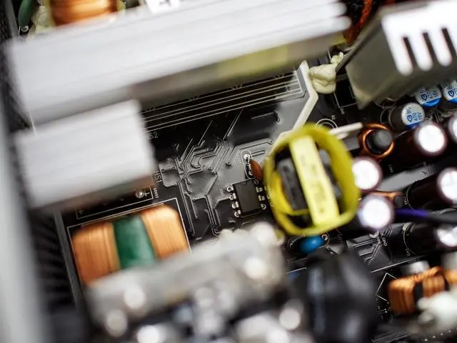
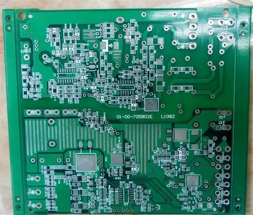
PCB board is the basIC electronic component of all electronic circuit design. As the main support, it carries all the components constituting the circuit. The role of PCB is not only to combine scattering elements, but also to ensure the regularity of circuit design and avoid confusion and errors caused by manual cables and wiring.
This paper introduces five key points of pcb board design in detail.
1. Have a reasonable direction
Such as input and output, AC and DC, strong and weak signals, high frequency and low frequency, high voltage and low voltage. Their directions should be linear (or separate) and should not be intertwined. Its purpose is to prevent mutual interference. The best direction is a straight line, but it is often difficult to achieve. The worst trend is rings. Fortunately, isolation can be improved. For DC, SMAll signal and low-voltage PCB boards, the design requirements can be lower. So "reasonable" is relative.
2. Choose a good grounding point: the grounding point is often the most important
I don't know how many engineers and technicians have discussed it, which shows its importance. Generally speaking, the foundation needs to be shared. For example, multiple ground wires of the preamplifier should be connected and then connected to the trunk line. In fact, it is difficult to fully implement various restrictions, but you should try to follow them. This question is very flexible in practice. Everyone has their own set of solutions. If it can be described for a specific circuit board, it can be easily understood.
3. Reasonably arrange decoupling capacitor of power filter
In general, only a few decoupling capacitors of power supply filter are drawn in the schematic diagram, but their connection positions are not indicated. In fact, these capacitors are used for switching devices (grids) or other components that require filtering and decoupling. These capacitors should be placed as close to these elements as possible, and they will be invalid if they are too far apart. Interestingly, when the decoupling capacitor of the power filter is correctly arranged, the problem of the grounding point is not obvious.
Wide line conditions should never be fined; High voltage and high frequency lines shall be smooth without sharp chamfers and corners shall not be used. The ground wire should be as wide as possible, and it is better to use a large area of copper, which can greatly improve the docking point problem. The pad or through hole size is too small, or the pad size does not match the hole size. The former is not suitable for manual drilling, while the latter is not suitable for numerical control drilling. It is easy to drill the pad into a "c" shape and then drill the pad. The wires are too thin and large areas of unrouted areas are free of copper, which may lead to uneven corrosion. That is, when the untwisted area is corroded, the thin wire may corrode too much, or it may be damaged or completely cracked. Therefore, the role of setting copper is not only to increase the ground area and anti-interference.
5. Number and linear density of via pcb solder joints
In the early stage of circuit production, some problems are not easy to find. They tend to appear at a later stage. For example, if there are too many holes, the copper sinking process will cause hidden dangers. Therefore, the design should minimize the number of holes. The straight lines in the same direction are too dense, which is easy to form a block during welding. Therefore, the linear density should be determined by the level of the welding process. the distance between the solder joints is too small, which is not conducive to manual welding. Otherwise, hidden dangers will be left. Therefore, the quality and work efficiency of welding personnel shall be taken into consideration when determining the minimum distance of welding points.
If you can fully understand and master the above PCB design considerations, you can b a lot of time and cost.


抖音二維碼

Q Q二維碼

微信二維碼
點擊
然后
聯系
然后
聯系
電話熱線
13410863085Q Q

微信

- 郵箱