鑫景福致力于滿足“快速服務,零缺陷,輔助研發”PCBA訂購單需求。


PCB制造
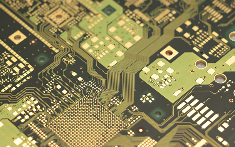
Surface treatment process of circuit board
How to select the surface treatment process of HASL, ENIG and OSP circuit boards?
After the PCB is designed, we need to choose the surface treatment process of the circuit board. Now the commonly used surface treatment processes of the circuit board include HASL (surface tin spraying process), ENIG (gold deposition process), OSP (oxidation prevention process). How should we choose the commonly used surface treatment process? Different PCB surface treatment processes have different charges, and the final results are different. You can choose according to the actual situation. Let me tell you about the advantages and disadvantages of HASL, ENIG, and OSP.
1. HASL (surface tin spraying process)
The tin spraying process can be divided into lead based and lead-free tin spraying. The tin spraying process was once the most important surface treatment process in the 1980s, but now, fewer and fewer circuit boards choose the tin spraying process, because the circuit boards are developing towards the "SMAll and refined" direction. The tin spraying process will lead to tin beads when fine components are welded, and poor production caused by spherICal tin dots, In order to pursue higher process standards and production quality, PCBA processing plants often choose ENIG and SOP surface treatment processes.
Advantages of lead spraying tin: low price, excellent welding performance, mechanical strength, glossiness, etc. are better than lead spraying tin.
Disadvantages of lead tin spraying: lead tin spraying contains lead heavy metals, which is not environmentally friendly in production and cannot pass ROHS and other environmental assesSMEnt.
Advantages of lead-free tin spraying: low price, excellent welding performance, and relatively environmental protection, can pass ROHS and other environmental evaluation.
Disadvantages of lead-free tin spraying: mechanical strength, glossiness, etc. are not as good as lead-free tin spraying.
Common disadvantage of HASL: It is not suitable for welding pins with thin gaps and too small components, because the surface flatness of tin spraying plate is poor. Tin beads are easy to be produced in PCBA processing, which is easy to cause short circuit to components with fine clearance pins.
2. ENIG
Gold deposition process is a relatively advanced surface treatment process, which is mainly used for circuit boards with connection functional requirements and long storage period.
Advantages of ENIG: It is not easy to oxidize, can be stored for a long time, and has a flat surface. It is suitable for welding thin gap pins and components with small solder joints. Repeated reflow soldering is not likely to reduce its solderability. It can be used as the base material for COB wiring.
Disadvantages of ENIG: the cost is high and the welding strength is poor. Because of the use of electroless nickel plating process, it is easy to have the problem of black disc. The nickel layer will be oxidized over time, and long-term reliability is a problem.
3. OSP (Anti oxidation Process)
OSP is an organic film formed chEMIcally on the bare copper surface. This film has oxidation resistance, heat shock resistance and moisture resistance to protect the copper surface from further rusting (oxidation or vulcanization, etc.) in normal environment; It is equivalent to an oxidation prevention treatment, but in the subsequent welding high temperature, the protective film must be easily removed by the flux, and the exposed clean copper surface can be immediately combined with the molten solder to form a solid solder joint in a very short time. At present, the proportion of circuit boards using the OSP surface treatment process has increased significantly, because this process is suitable for both low process circuit boards and high process circuit boards. If there is no functional requirement for surface connection or storage period limitation, the OSP process will be the most ideal surface treatment process.
Advantages of OSP: It has all the advantages of bare copper plate welding. The expired (three months) plates can also be resurfaced, but usually only once.
Disadvantages of OSP: It is easily affected by acid and humidity. When it is used for the second reflow soldering, it needs to be completed within a certain time, and the effect of the second reflow soldering is usually poor. If the storage time exceeds three months, the surface must be re treated. Use up within 24 hours after unpacking. OSP is an insulating layer, so the test point must be printed with solder paste to remove the original OSP layer before contacting the pin point for electrical test. The assembly process needs to be greatly changed. If the unprocessed copper surface is detected, it will be bad for ICT. If the over sharp ICT probe may damage the PCB, manual preventive treatment is required, which limits ICT testing and reduces the repeatability of testing.
The above is about the analysis of the surface treatment process of HASL, ENIG and OSP circuit boards. You can choose which surface treatment process according to the actual use of circuit boards.


抖音二維碼

Q Q二維碼

微信二維碼
點擊
然后
聯系
然后
聯系
電話熱線
13410863085Q Q

微信

- 郵箱