鑫景福致力于滿足“快速服務,零缺陷,輔助研發”PCBA訂購單需求。


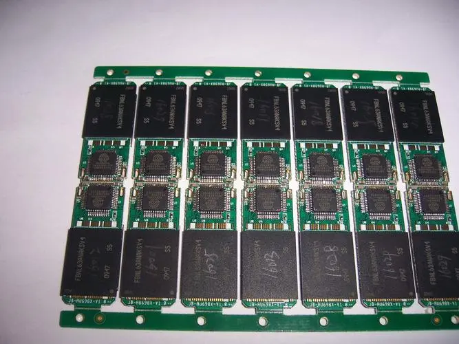
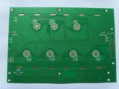
PCB制造
1、 PCB layout
1. PCB layout refers to the reasonable layout of PCB components. What kind of placement is reasonable. A SIMple principle is the clear division of modules. In other words, people with a certain circuit foundation can see whICh printed circuit board is used to achieve what functions.
2. SpecifIC design steps: first, generate the initial PCB file according to the schematic diagram, complete the pre layout of the PCB, determine the relative PCB layout area, then tell the structure that the structure is based on the area we give, and then give specific constraints according to the overall structure design.
3. According to the structural constraints, complete the drawing of plate edges, positioning openings and some prohibited areas, and then complete the placement of connectors
4. Element placement principle: Generally, the main control microcontroller (MCU) is placed in the center of the circuit board, and then the interface circuit is placed close to the interface (such as network port, USB, VGA, etc.), Most interfaces have ESD protection and filtering functions. The principle to follow is to protect before filtering.
5. Then the power module. Generally, the main power module is placed at the power inlet (such as 5V of the system). Independent power modules (such as 2.5V provided by module circuit) can be placed in densely populated places in the same power supply network according to the actual situation.
6. Some internal circuits are not connected to connectors. We usually follow such a basic principle: high-speed and low-speed partition, analog and digital partition, interference source and sensitive receiver partition.
7. Then, for a single circuit module, design according to the current flow direction during circuit design.
The whole circuit layout is like this. You are welcome to add and correct it.
2、 Wiring
1. The basic requirement for cabling is to ensure the effective connection of all networks. Connectivity is easy to do, and validity is a vague concept. In fact, there are only two kinds of signals in the circuit: digital signal and analog signal. For digital circuits, it is to ensure adequate noise tolerance, while for analog signals, it is to achieve zero loss as far as possible.
2. Before wiring, it is usually necessary to understand the laminated design of the entire printed circuit board, that is, plan all PCB wiring layers as: the best wiring layer and the next best wiring layer...., The optimal wiring layer, i.e. the adjacent complete ground plane, is generally used to distribute important signals (including all signals, differential signals, analog signals, etc. in DDR). Other signals (I2C, UART, SPI, GPIO) pass through other layers, and only relevant signals of this circuit (such as DDR, network port, etc.) are ensured It exists in important areas.
3. Reflection, crosstalk, electromagnetic compatibility and other issues need to be considered in high-speed signal wiring, so impedance matching is generally required, such as single line 50R, differential line 100R, etc. The actual design shall prevail (the principle is to ensure equal and continuous impedance). Crosstalk mainly considers 3W/2W principle, group grounding treatment, etc.
4. The power supply and power circuit shall first ensure sufficient bearing capacity, that is, the whole circuit of the power supply shall be as thick and short as possible. From the perspective of electromagnetic compatibility, the echo is calLED loop, forming loop antenna and radiating outwards, so as to minimize the loop area
The overall wiring of the circuit is like this, welcome the great God to add and correct.
3、 Land
1. Grounding and grounding design are very important in PCB design, because grounding is an important reference plane. If there is a problem with the ground plane design, other signals cannot be stabilized.
2. Generally, we can divide it into chassis grounding and system grounding. As the name implies, chassis grounding is the grounding connected by product metal chips, and system grounding is the reference plane of the entire circuit system.
3. The practical principle of the general system and cabinet is that the cabinet is divided into grounding and system, and then connected to the high-voltage capacitor through magnetic beads or multipoint.
4. On the system: in terms of function, it is divided into digital, analog and power supply. There has been a dispute about the division of land. I come from here
First of all, I think the land can be divided when the PCB layout is very reasonable. The meaning of PCB layout is very reasonable, that is, there are only digital signals in the digital area, only analog signals in the analog area, and only power signals in the power area. There is a complete ground plane below. Because the current is very similar to the current, they all flow downward, and there is a complete ground plane below them. Therefore, starting from the principle of the shortest and lowest, they flow directly back below and will not escape to other places.
The whole process of PCB copying
10-27,2022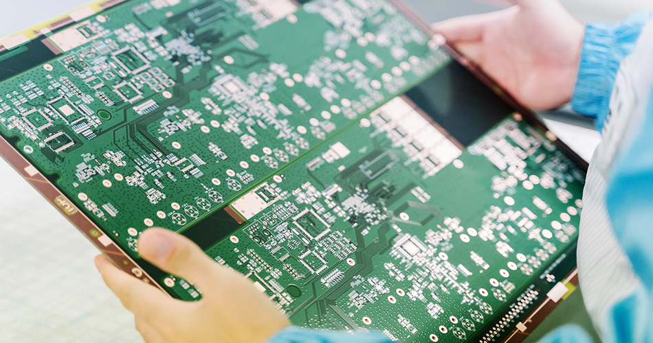


抖音二維碼

Q Q二維碼

微信二維碼
點擊
然后
聯系
然后
聯系
電話熱線
13410863085Q Q

微信

- 郵箱