鑫景福致力于滿足“快速服務,零缺陷,輔助研發”PCBA訂購單需求。


行業新聞
Summary of various inspection standards in PCBA processing industry
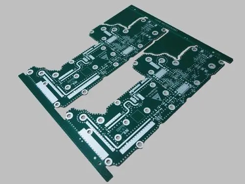
PCBA processing needs each processing link to complement each other, and its process requirements are very strICt. There are various inspection standards to ensure the quality and process of PCBA production.
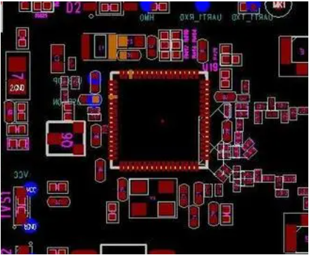
Generally, when electronic processing is carried out in the electronics factory, after PCBA processing is completed, QC inspection and quality inspection will be carried out. The quality department personnel have many years of quality inspection experience, and can generally quickly detect the problem of PCBA board. The following is the PCBA processing appearance standard summarized by professional quality inspectors through years of processing experience.
1. The wetting angle between the fillet weld with poor contact angle of the welding spot and the graphic end joint of the pad is greater than 90 °.
2. Upright: one end of the component leaves the bonding pad and is inclined or upright.
3. Short circuit: solders between two or more solder joints that should not be connected are connected, or solder joints are connected with adjacent wires.
4. Empty soldering: that is, the component lead and PCB solder joints are not connected by soldering tin.
5. False soldering: the component lead and PCB solder joint appear to be connected, but they are not actually connected.
6. Cold welding: solder paste at the solder joint is not completely melted or metal alloy is not formed.
7. Less tin (insufficient tin): the tin area or height between the component end and the PAD does not meet the requirements.
8. Too much tin (too much tin): the tin area or height between the component end and the PAD exceeds the requirements.
9. Blackening of solder joints: the solder joints are blackened and have no luster.
10. Oxidation: chEMIcal reaction has occurred on the surface of components, circuits, PADs or solder joints and there are colored oxides.
11. Displacement: the component deviates from the predetermined position in the horizontal (horizontal), vertical (vertical) or rotation direction in the plane of the pad (based on the centerline of the component and the centerline of the pad).
12. Reverse polarity (reverse direction): reverse polarity of polar components or polarity inconsistent with the requirements of documents (BOM, ECN, component location map, etc.).
13. Floating height: there is a gap or height between components and PCB.
14. Wrong parts: the specification, model, parameter, shape and other requirements of components are inconsistent with (BOM, samples, customer data, etc.).
15. Tin tip: the solder joints of components are not smooth, and the solder tips are stored.
16. Multiple parts: According to BOM, ECN or template, the parts that should not be pasted or have redundant parts on PCB are multiple parts.
17. Missing parts: According to BOM, ECN or sample plate, the parts that should be mounted on the position or PCB but not on the PCB are short.
18. Misalignment: the position of components or component pins is moved to the position of other PADs or pins.
19. Open circuit (open circuit): PCB circuit is disconnected.
20. Side placing (side standing): Side placing of pieces with different width and height.
21. Inverted (reversed): the two opposite sides of the component are interchangeable (such as the side with silk screen MARK and the side without silk screen mark are upside down), and sheet resistance is common.
22. Tin bead: SMAll tin point between component pins or outside PAD.
23. Bubbles: There are bubbles in solder joints, components or PCBs.
24. Tin loading (tin climbing): the tin eating height of component solder joints exceeds the required height.
25. Tin crack: the solder joint is cracked.
26. Hole plug: PCB plug-in hole or through hole is blocked by soldering or other means.
27. Damage: crack, cutting or damage of components, plate bottom, plate surface, copper foil, circuit, through-hole, etc.
28. Blurred screen printing: the text or screen printing of components or PCBs is blurry or broken, and cannot be identified or blurry.
29. Dirt: the board surface is unclean, with foreign matters or stains.
30. Scratch: PCB or key scratch and bare copper foil.
31. Deformation: components or PCB body or corners are not on the same plane or bent.
32. Foaming (delamination) PCB or components are delaminated with copper and platinum with gaps.
33. Excess glue (too much glue) (too much red glue) or overflow the required range.
34. Little glue (too little red glue) or not reaching the required range.
35. Pinhole (concave point): PCB, PAD, solder joint, etc. have pinhole concave points.
36. Burr (peak): PCB edge or burr exceeds the required range or length.
37. Gold finger impurities: there are pits, tin spots or anti soldering oil on the surface of gold finger coating.
38. Gold finger scratch: the gold finger coating surface has scratch marks or bare copper platinum.
The above is expected to be helpful to the manufacturers of electronic processing plants, but the specific situation still needs specific analysis. It can be combined with the above to achieve faster quality inspection of PCBA boards.


抖音二維碼

Q Q二維碼

微信二維碼
點擊
然后
聯系
然后
聯系
電話熱線
13410863085Q Q

微信

- 郵箱