鑫景福致力于滿足“快速服務,零缺陷,輔助研發”PCBA訂購單需求。


行業新聞
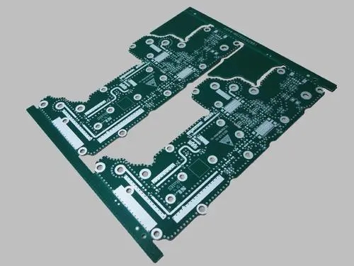
Stacking design Method of Balanced PCB boards
Designers can design an odd PCB If routing does not require additional layers, why use it? Won't reducing the number of layers make the board thinner? If there is one less circuit board, wouldn't the cost be lower? However, in some cases, adding a layer can actually reduce costs The circuit board has two different structures: core structure and foil structure In the core structure, all conductive layers in the circuit board are coated on the core material; In the foil structure, only the internal conductive layer of the circuit board is coated on the core material, and the external conductive layer is coated with the foil coated dielectrIC plate All conductive layers are bonded together by a multilayer lamination process using dielectrics The nuclear material is the factory's double-sided foil Because each core has two sides, when fully utilized, the number of conductive layers on the PCB is uniform Why not use the foil on one side and use the core structure for the rest? The main reason is PCB board and PCB board
PCB board

Cost advantages of even laminates
Since there are fewer dielectric and foil layers, the raw material cost of odd PCB is slightly lower than that of even PCB. However, the processing cost of odd PCB is significantly higher than that of even PCB. The processing cost of the inner layer is the same; However, the foil/core structure significantly increases the processing cost of the outer layer. Singular layer PCB needs to add non-standard laminated core layer welding process on the basis of core structure process. Compared with the core structure, the factory adding foil outside the core structure will lose productivity. Before laminated bonding, the outer core needs additional treatment, which increases the risk of scratches and etching errors in the outer layer.
Balanced structure to avoid bending
The reason why PCB with odd layers is not designed is that odd layers are easy to bend. When the PCB is cooLED after the multi-layer circuit bonding process, the different laminating tensions of the core structure and the foil covering structure will cause the PCB to bend. As the thickness of the board increases, the risk of bending composite PCB boards with two different structures increases. The key to eliminating board flex is balanced stacking. Although PCB boards with a certain curvature meet the requirements of the specification, the subsequent processing efficiency will be reduced, resulting in additional costs. Due to the special equipment and process required for assembly, the accuracy of placement of this part will be reduced, thus affecting the quality.
Use evenly layered PCBs
When odd PCB boards appear in the design, the following methods can be used to achieve balanced stacking, reduce PCB manufacturing costs, and avoid PCB bending. The following methods are listed in order of priority.
1) A signal layer and use. This method can be used if the power supply layer of the PCB board is even and the signal layer is odd. The added layers will not increase the cost, but can shorten the lead time and improve the quality of PCB.
2) Add additional power layers. This method can be used if the power plane of the design PCB is odd and the signal plane is even. A SIMple way is to add a formation in the middle of the stack without changing other settings. First, route the PCB according to the odd number of layers, then copy the middle ground plane and MARK the remaining layers. This is the same as the electrical characteristics of the thickened foil.
3) Add a blank signal layer near the center of the PCB stack. The method eliminates the stacking imbalance and improves the quality of PCB. First route the odd numbered layers, then add a blank signal layer and mark the remaining layers. It is used in microwave circuit and mixed medium (medium with different dielectric constant) circuit.
Advantages of balanced lamination PCB board: low cost, not easy to bend, short delivery time, and guaranteed quality
The above is the explanation given by the editor of pcb circuit board company. If you want to know more about PCBA, you can go to our company's home page to learn about it. In addition, our company also sells various circuit boards,
High Frequency Circuit Board and SMT chip are waiting for your presence again.
Some small principles of PCB technology
11-04,2022


抖音二維碼

Q Q二維碼

微信二維碼
點擊
然后
聯系
然后
聯系
電話熱線
13410863085Q Q

微信

- 郵箱