鑫景福致力于滿足“快速服務,零缺陷,輔助研發”PCBA訂購單需求。


行業新聞

Anti interference design principle of PCB board
PCB board supports circuit components and devICes in electronic products It provides electrical connections between circuit components and equipment With the rapid development of electronic technology, the density of PGB is getting higher and higher The anti-interference ability of quality PCB design has great influence Therefore, in the design of PCB board General principles PCB board must follow the design and meet the requirements of anti-interference design General principles PCB board design is to obtain the efficiency of electronic circuits. Component layout and wire layout are very important In order to design a PCB board with good quality and low cost
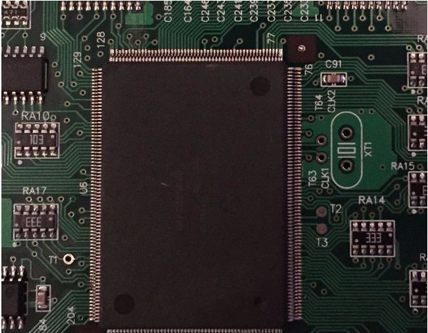
PCB board

1. Layout first, and consider PCB board When the PCB board is too large, the printed lines will be very long, the impedance will be increased, the noise resistance will be reduced, and the cost will be increased; If the size is too SMAll and the heat dissipation is poor, adjacent lines are prone to interference After determining the PCB board Then determine the location of the special components, Layout of all components of the circuit according to the functional unit of the circuit When locating special components, follow these guidelines:
1) Shorten the connection between high-frequency components as much as possible, and minimize their distribution parameters and mutual electromagnetic interference. Components susceptible to interference shall not be too close to each other, and input and output components shall be as far away as possible.
2) There may be high potential difference between some components or wires, and the distance between them shall be increased to avoid accidental short circuit caused by discharge. High voltage components shall be arranged in places that are not easy to touch during commissioning.
3) Components weighing more than 15g shall be fixed with brackets and then welded. Those large, heavy components that generate a lot of heat should not be instalLED on the printed board, but should be installed on the chassis backplane of the entire machine, and heat dissipation should be considered. The heating element shall be far away from the heating element.
4) For the layout of adjustable components such as potentiometers, adjustable inductance coils, variable capacitors and microswitches, the structural requirements of the whole machine shall be considered. If the adjustment is made inside the machine, it should be placed on the printed board to facilitate the adjustment; If the adjustment is carried out outside the machine, its position should match the position of the adjustment knob on the chassis panel.
5) The position occupied by the positioning hole of the printing pulley and the fixing bracket shall be reserved. According to the functional unit of the circuit. The following principles shall be followed when arranging all components of the circuit:
Arrange the position of each functional circuit unit according to the circuit flow, so that the layout is convenient for the signal flow and the signal is kept in the same direction as far as possible.
B Layout around each functional circuit element centered on it. Elements shall be evenly, neatly and compactly arranged on PCB. Minimize and shorten wires and connections between assemblies.
C For the circuit working at high frequency, the distribution parameters between elements shall be considered. In general circuits, elements shall be arranged in parallel as far as possible. This is not only beautiful. It is easy to install and weld. Easy to mass produce.
D The distance between the components at the edge of the circuit board and the edge of the circuit board is usually not less than 2mm. The shape of the circuit board is rectangular. When the size of the circuit board is larger than 200x150mm, the aspect ratio is 3:2 to 4:3. The mechanical strength of the circuit board shall be considered.
2. Wiring;
1) The wires used on the input and output terminals shall be avoided adjacent and parallel as far as possible. Add ground wires between wires to avoid reverberation coupling.
2) The width of the printed wire is mainly determined by the adhesion strength between the wire and the insulating substrate and the current value flowing through them. When the thickness of copper foil is 0.05mm and the width is 1-15mm. When the current is 2A, the temperature will not be higher than 3 ° C. 1.5mm line width can meet the requirements. For integrated circuits, especially digital circuits, 0.02-0.3mm line width is usually selected. Of course, use as wide a line as possible. Especially the power line and ground wire. The wire spacing is mainly determined by the insulation resistance between wires and the breakdown voltage under adverse conditions. For integrated circuits, especially digital circuits, as long as the process allows, the spacing can be as small as 5-8mm.
3) The angle of printed conductor is usually arc-shaped, and right angle or included angle will affect the power efficiency in high-frequency circuit. In addition, try to avoid using large area copper foil, otherwise the copper foil is easy to expand and fall off when heated for a long time. When large area copper foil must be used, please use grating. This is beneficial to eliminate the volatile gas generated by heating the adhesive between the copper foil and the substrate.
3. The center hole of the pad is slightly larger than the diameter of the device lead. If the pad is too large, it is easy to form virtual solder. The outer diameter D of the gasket is usually not less than (D+1.2) mm, where D is the diameter of the lead hole. For high-density digital circuits, the diameter of the pad may be (d+1.0) mm. Anti interference measures of PCB and circuit Anti interference design of PCB is closely related to specific circuit.
3.1 The power line shall be designed according to the current of the printed circuit board, and the width of the power line shall be increased as much as possible to reduce the circuit resistance. At the same time, make the direction of the power cord and ground wire consistent with the direction of data transmission, which will help to enhance the anti noise capability.
3.2 The ground line design principles for plot design are:
1) Separate digital grounding from analog grounding. If there are logic circuits and linear circuits on the circuit board, they should be separated as far as possible. The grounding of low frequency circuit shall be connected in parallel at single point as far as possible. When the actual wiring is difficult, part of it can be connected in series and then connected to the ground in parallel. High frequency circuit shall be grounded at multiple points in series, the grounding wire shall be short circuited and leased, and large area grid grounding foil shall be used around high-frequency components as far as possible.
2) The grounding wire shall be as thick as possible. If the grounding wire is very thin, the grounding potential will change with the change of current, which will reduce the anti noise efficiency. In this case, the ground wire should be thickened so that it can pass the current on the printed board 3 tiMES the allowable current. If possible, the ground wire should be larger than 2-3 mm.
3) The ground wire forms a closed loop. For printed boards composed of digital circuits only, most grounding circuits are arranged in the loop, which can improve the anti noise ability.
3.3 One of the traditional methods in PCB design for decoupling capacitors is to include appropriate decoupling capacitors in each key part of the PCB. The general configuration principles of decoupling capacitors are:
1) Connect a 10~100uf electrolytic capacitor at the power input end. If possible, it is better to connect more than 100uF.
2) In principle, each integrated circuit chip shall be equipped with a 0.01pF ceramic capacitor. If the space of the printed board is insufficient, a 1~10pF capacitor can be arranged every 4~8 chips.
3) For devices with weak noise resistance and large power change when turned off, such as RAM and ROM storage devices, decoupling capacitors should be directly connected between the power line and ground wire of the chip.
4) The lead wire of the capacitor should not be too long In addition, pay attention to the following two points: when there are contactors, relays, buttons, and other component PCB boards
The above is the explanation given by the editor of pcb circuit board company. If you want to know more about PCBA, you can go to our company's home page to learn about it. In addition, our company also sells various circuit boards,
High Frequency Circuit Board and SMT chip are waiting for your presence again.


抖音二維碼

Q Q二維碼

微信二維碼
點擊
然后
聯系
然后
聯系
電話熱線
13410863085Q Q

微信

- 郵箱