鑫景福致力于滿足“快速服務,零缺陷,輔助研發”PCBA訂購單需求。


行業新聞
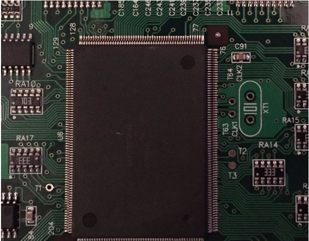
The design of printed circuit board mainly refers to layout design, whICh needs to consider the layout of external connections. Optimized layout of internal electronIC components. Optimized layout of metal wiring and through-hole. Electromagnetic protection. Heat dissipation and other factors.
When designing PCB (printed circuit board), one of the most basic issues to consider is how many wiring layers, grounding planes and power planes are required to achieve the required functions of the circuit. The determination of the number of layers of wiring layers, grounding planes and power planes of the printed circuit board is related to the requirements of circuit function, signal integrity, EMI, EMC, manufacturing cost, etc. For most designs, there are many conflicting requirements for factors such as PCB performance requirements, target cost, manufacturing technology and system complexity, etc. The stack design of PCB is usually a compromise after considering various factors. Digital circuits and transmitter circuits are usually designed with multilayer boards.
Guangzhou high-speed PCB design
The following lists 8 principles for stack design:
1. Layering
In a multilayer PCB, it usually includes a signal layer (S), a power supply (P) plane, and a ground (GND) plane. The power plane and ground plane are usually undivided solid planes, which will provide a good low impedance current return path for the current of adjacent signal lines. Most of the signal layers are located between these power or ground reference plane layers, forming symmetrical striplines or asymmetrical striplines. The top and bottom layers of multilayer PCB are usually used to place components and a SMAll amount of wiring. These signal wiring should not be too long to reduce the direct radiation generated by wiring.
2. Determine the single power reference plane (power plane)
Using decoupling capacitor is an important measure to solve the integrity of power supply. The decoupling capacitor can only be placed on the top and bottom layers of the PCB. The wiring, bonding pad and via of decoupling capacitor will seriously affect the effect of decoupling capacitor, which requires that the wiring connecting decoupling capacitor should be as short and wide as possible, and the wire connected to via should also be as short as possible. For example, in a high-speed digital circuit, the decoupling capacitor can be placed on the top layer of the PCB, the second layer is allocated to the high-speed digital circuit (such as the processor) as the power layer, the third layer is used as the signal layer, and the fourth layer is set as the high-speed digital circuit ground.
In addition, it is necessary to ensure that the signal wiring driven by the same high-speed digital device takes the same power supply layer as the reference plane, and this power supply layer is the power supply layer of high-speed digital devices.
3. Determine the multi power reference plane
The multi power reference plane will be divided into several solid regions with different voltages. If the signal layer is close to the multiple power supply layer, the signal current on the signal layer near it will encounter an undesirable return path, causing gaps in the return path. For high-speed digital signals, this unreasonable return path design may cause serious problems, so high-speed digital signal wiring should be far away from the multi power reference plane.
4. Determine multiple ground reference planes (ground plane)
Multiple ground reference planes (ground planes) can provide a good low impedance current return path, which can reduce the common mode EMl. The ground plane and the power plane should be closely coupLED, and the signal layer should also be closely coupled with the adjacent reference plane. This can be achieved by reducing the thickness of the medium between layers.
5. Reasonably design wiring combination
The two layers crossed by a signal path are called a "wiring combination". The best wiring combination design is to avoid the return current flowing from one reference plane to another, but from one point (face) of one reference plane to another. In order to complete the complex cabling, the inter layer conversion of routing is inevitable. During signal layer to layer conversion, it is necessary to ensure that the return current can flow smoothly from one reference plane to another. In a design, it is reasonable to take the adjacent layer as a wiring combination. If a signal path needs to span multiple layers, it is usually not a reasonable design to take it as a wiring combination, because a path passing through multiple layers is not smooth for the return current. Although the ground spring can be reduced by placing decoupling capacitors near the vias or reducing the dielectric thickness between reference planes, it is not a good design.
6. Set wiring direction
On the same signal layer, it shall be ensured that the direction of most wiring is consistent and orthogonal to the wiring direction of adjacent signal layers. For example, you can set the wiring direction of one signal layer as the "Y axis" direction, and set the wiring direction of another adjacent signal layer as the "X axis" direction.
7. Even layer structure
It can be found from the designed PCB stack that the classical stack design is almost all even layers, not odd layers. This emergency is caused by a variety of factors, as shown below.
It can be learned from the manufacturing process of printed circuit board that all conductive layers in the circuit board are saved on the core layer. The core layer is usually made of double-sided cladding. When the core layer is fully used, the conductive layers of the printed circuit board are even.
Even layer printed circuit board has cost advantage. The cost of raw materials of odd layer PCB is slightly lower than that of even layer PCB due to the lack of one layer of dielectric and copper coating. However, because the odd layer PCB needs to add non-standard laminated core bonding process on the basis of core structure process, the processing cost of odd layer PCB is significantly higher than that of even layer PCB. Compared with the ordinary core structure, adding copper coating outside the core structure will lead to the decline of production efficiency and the extension of production cycle. Before laminating and bonding, the outer core layer needs additional PCB processing, which increases the risk of outer layer being scratched and wrongly etched. The additional coating treatment will greatly increase the manufacturing cost.
When the inner and outer layers of a printed circuit board are cooled after the multilayer circuit bonding process, different laminating tensions will make the printed circuit board bend to varying degrees. And with the increase of PCB thickness, the risk of bending of composite PCB with two different structures is greater. The odd layer PCB is easy to bend, while the even layer PCB can avoid bending.
In the design, if there are odd layers, the following method can be used to increase the number of layers.
If the power supply layer of the printed circuit board is even and the signal layer is odd, the method of increasing the signal layer can be adopted. The added signal layer will not increase the cost, but can shorten the processing time and improve the quality of printed circuit board.
If the power supply layer of the printed circuit board is odd and the signal layer is even, the method of increasing the power supply layer can be adopted. Another SIMple method is to add a ground plane in the middle of the stack without changing other settings, that is, first wire the PCB in odd layers, and then copy a ground plane in the middle.
In microwave circuits and mixed dielectric circuits (the dielectric has different permittivity), a blank signal layer can be added near the center of the PCB stack to minimize stack imbalance.


抖音二維碼

Q Q二維碼

微信二維碼
點擊
然后
聯系
然后
聯系
電話熱線
13410863085Q Q

微信

- 郵箱