鑫景福致力于滿足“快速服務,零缺陷,輔助研發”PCBA訂購單需求。


行業新聞
USB3.0 can provide a data rate of up to 5Gbps, ten tiMES faster than high-speed USB (USB2.0), and has improved power effICiency. At this high transmission speed, the signal integrity problem is increasingly limiting the PCB routing, PCB wiring length and its design and implementation functions. Poor signal quality may seriously affect system performance and reliability. The USB3.0 ReDriverSuperspeed in terminal equipment application is a dual channel memory (TX ± and RX ±), multi-channel USB3.0 docking driver, which is used for notebook, desktop computer, docking station, side panel, cabling and other terminal equipment applications. Each secure channel provides selectable balance settings to compensate for different input wiring losses.
USB3.0 Design Manual
1. It is proposed to place 0.1uF decoupling capacitor on each VDD pin of IC for VDD decoupling capacitor. Below is the reference for the reasonable layout of the coupling capacitor placement on the circuit board. The four pink round decoupling capacitors at the bottom are located around the four VDD pins (pins 6, 10, 16 and 20) of the IC.
2. The PCB layer is proposed to use at least four layers of PCB for USB3.0 design. Each data information signal trace shall be completely routed on the ground plane of adjacent layers to meet the requirements of characteristic impedance measurement.
3. Route the cable along the USB connector.
The USB socket connector applied to the PCB when designing the motherboard. For Vbus routing, it is proposed to insert ferrite beads. For the shielding of USB connector (shielding of USB cable), AC is isolated from ground (such as the moderate value of inductance, instead of connecting the signal wire shielding layer to the PCB grounding structure immediately).
For USB3.0 signal routing, the characteristic impedance shall be maintained. Prevent cross cutting and removing any cabling that causes intermittent signals and serious EMC noise problems. In addition, when the application pin is inserted into the PCB, do not place any isolation between all USB3.0 signal pairs of each layer.
Crosstalk between signal lines
USB3.0 has three pairs of signals (SSTX ±/SSRX ±/D ±)
There are three typical types of far end crosstalk:
SSTX ± to D ± in RX mode
SSTX ± to SSRX ±
D ± to SSRX ± in TX mode
In order to minimize crosstalk, the wiring of SSTX ±/SSRX ± and D ± to the intermediate signal wiring cannot be closed to each other. USB3.0 signal wiring characteristic impedance The reasonable layout around the USB3.0 socket connector is placed as one or several reference planes in a special layer (such as GND layer). In order to maintain the differential characteristic impedance of high-speed signal wiring, please ensure that there is no copper cutting between the pins of any differential pair. The GND layer of the second layer of USB3.0 is hollowed out, and the SS signal differential pair is designed in the upper layer, which will cause the problem of signal discontinuity, and the pin position on the USB3.0 socket connector will become a stub of the approach.
4. Wiring tightly around USB controller
Because the high-speed signal is sensitive to the switching power supply signal, the reasonable layout of the switching power supply and grounding device of the USB controller must be careful. As for Part (A), each switch power supply pin must be decoupLED with a capacitor, which should be close to the switch power supply pin of the USB controller as far as possible. Because USB controller includes analog and digital parts, it must be analog switching power supply and digital switching power supply system. In order to prevent common faults of digital integrated circuits caused by digital signal interference, attention should be paid to the isolation between analog switching power supply and digital signal wiring (including signal wiring). For analog power and digital power of the same voltage level, ferrite beads shall be added during the period for noise filtering.
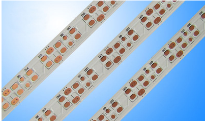
Usb circuit board
Summary
Reasonable PCB layout design:
The USB controller and USB connector should be as close as possible to reduce the length of the cable. Magnetic beads and decoupling capacitors used for decoupling and removing high frequency noise interference should be placed as close to the USB connector as possible.
The matching resistor of the terminal device should be placed at the end close to the USB controller.
The voltage regulator should also be placed as close to the connector as possible.
Wiring design:
The routing length shall be reduced as far as possible. The wiring of high-speed USB differential line shall be given priority, and the high-speed USB differential line, any connector and digital signal line with steep edge shall be prevented from approaching the routing as far as possible.
Try to reduce the number of vias and corners on the USB high-speed signal line, so as to better ensure the manipulation of characteristic impedance and prevent signal reflection.
It is strictly prohibited to use 90 ° routing angle, and use two forty-five degrees to achieve turning or an arc to achieve turning, which will greatly reduce the signal reflection and the discontinuity of characteristic impedance.
Do not walk the signal line under the IC with crystal oscillator circuit, crystal, clock synthesizer, magnetic element device and clock memory overclocking.
Short stake lines (stubs) shall be prevented on the signal line, otherwise the signal may be reflected and the signal integrity may be affected. If short pile line is unavoidable, its length shall not exceed 50mils.
Try to run the high-speed signal lines in the same layer. Ensure that there is a detailed unshared image plane (VCC or GND, select GND plane first) for the return relative path of the routing. If possible, do not exceed the split line of the mirror image plane (such as the split line of different switching power supplies on the switching power supply plane), otherwise the self inductance coefficient may be increased and the signal radiation may be expanded.
The differential signal lines are routed side by side.
Differential signal wiring
The wiring spacing between parallel USB differential signal pairs shall ensure the differential characteristic impedance of 90 ohms.
Reduce the length of high-speed USB signal line, high-speed clock line and AC signal line side by side, or increase their spacing side by side to reduce the impact of crosstalk. The distance between differential pair signal and other signal wiring shall be at least 50 mils.
The tight coupling mode is selected in the middle of differential pair signals, that is, the distance between the lines is lower than the total width of the lines, which can improve the working ability of differential signals against external noise interference. The actual cable spacing and total width must be determined according to the relevant mobile phone software.
For differential signal, it is better to ensure that the distance between the two routes is consistent everywhere and the length matches. Its large length difference (such as the length difference between DP and DM) cannot exceed 50mils.
The length matching is more critical than keeping the spacing consistent everywhere. Therefore, the length matching is preferred to ensure that the signal wiring can be wound in some places where the wiring spacing cannot be kept consistent to ensure the consistent length of the two PCB wiring.


抖音二維碼

Q Q二維碼

微信二維碼
點擊
然后
聯系
然后
聯系
電話熱線
13410863085Q Q

微信

- 郵箱