鑫景福致力于滿足“快速服務,零缺陷,輔助研發”PCBA訂購單需求。


行業新聞

The surface of LED display circuit board has several processing PCB processes: light board (without any surface treatment), rosin board, OSP (organIC solder protective agent, slightly better than rosin), tin spraying (with or without lead tin), gold plated board, gold plated board, etc.
Difference between Gold Deposition Process and Gold Plating Process
Gold plated plate: golden and white, poor welding, skin effect is not conducive to high-frequency signal transmission,
Disadvantages: The gold surface is easy to be oxidized, and the gold wire is easy to be short, and the welding adhesion is not strong.
: golden yellow, good weldability, skin effect has no effect on signal.
Advantages: It is not easy to oxidize, does not produce gold wire, and has good resistance to welding.
The method of chEMIcal deposition is adopted for gold deposition. A layer of coating is generated by chemical oxidation and reduction reaction, which is generally thicker. It is one of the methods of chemical nickel gold gold deposition, and can reach a thicker gold layer.
Gold plating is based on the principle of electrolysis, also known as electroplating. Other metal surface treatment also mostly adopts electroplating.
In the actual product application, 90% of the gold plates are gold plated plates. Because the poor weldability of the gold plated plates is his fatal disadvantage, it is also the direct reason that many companies give up the gold plating process!
The gold deposition process deposits nickel gold coating with stable color, good brightness, flat coating and good solderability on the surface of printed circuit. It can be basically divided into four stages: pretreatment (degreasing, micro etching, activation, post leaching), nickel precipitation, gold precipitation, and post-treatment (waste gold washing, DI washing, drying). The thickness of gold deposit is 0.025-0.1um.
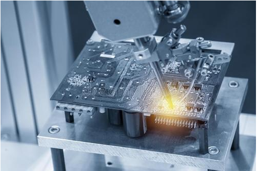
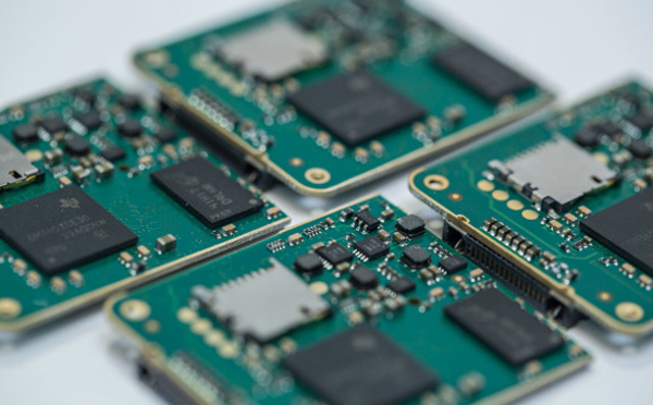
Display circuit board
The display circuit board gold should be used for the surface treatment of the circuit board. Because of its strong conductivity, good oxidation resistance and long service life, gold is generally used in such applications as key boards, gold finger boards, etc. The fundamental difference between gold plated boards and gold plated boards is that gold plated is hard gold (wear-resistant) and gold plated is soft gold (non wear-resistant).
1. The crystal structure formed by gold deposition is different from that formed by gold plating. The thickness of gold deposition is much thicker than that of gold plating. The gold deposition will be golden yellow, which is more yellow than gold plating (this is one of the methods to distinguish gold plating from gold deposition), and the gold plating will be slightly white (the color of nickel).
2. The crystal structure formed by gold deposition is different from that formed by gold plating. Compared with gold plating, gold deposition is easier to weld and will not cause poor welding. The stress of the gold plate is easier to control, which is more conducive to the processing of bonding products. At the same time, it is precisely because the gilt is softer than the gilt, so the gilt finger made of the gilt plate is not wear-resistant (the disadvantage of the gilt plate).
3. Only the bonding pad of the gold plated plate has nickel gold, and the signal transmission in the skin effect will not affect the signal in the copper layer.
4. The crystal structure of gold deposit is denser than that of gold plating, and it is not easy to produce oxidation.
5. With the increasing requirement of PCB processing accuracy, the line width and spacing have reached below 0.1mm. Gold plating is easy to cause gold wire short circuit. Only the bonding pad of the gold plate has nickel gold, so it is not easy to produce gold wire short circuit.
6. Only the PCB pad of the gold plated board has nickel gold, so the solder resistance on the circuit is more firmly combined with the copper layer. The project will not affect the spacing when making compensation.
7. For boards with higher requirements, the flatness is required to be better. Generally, the method of gilding is adopted, and the phenomenon of black pad after assembly will not occur. The flatness and service life of the gold plated plate are better than those of the gold plated plate.
So at present, most PCB factories adopt the gold deposition process to produce gold plates. However, the gold deposition process is more expensive than the gold plating process (higher gold content), so there are still a large number of low-cost products using the gold plating process.


抖音二維碼

Q Q二維碼

微信二維碼
點擊
然后
聯系
然后
聯系
電話熱線
13410863085Q Q

微信

- 郵箱