鑫景福致力于滿足“快速服務(wù),零缺陷,輔助研發(fā)”PCBA訂購單需求。


行業(yè)新聞
Through practICe and exploration, we will find that there are rules to follow. The following will discuss the circuit board design of RF circuits around these aspects: layout, impedance, lamination, design considerations, edging, power treatment, and surface treatment based on our years of work experience and previous experience.
1 About PCB layout
The principle of RF circuit layout is that the RF signal should be as short as possible, and the input should be far away from the output. RF lines should preferably be arranged in a straight line, followed by an L-shaped layout, or an obtuse angle greater than 90 degrees (such as 135 degrees). There is also a U-shaped layout, which mainly depends on the space and wiring needs. The U-shaped layout is used when conditions are really limited, and the distance between two parallel lines should be at least 2mm. High sensitive devices such as filters need to be equipped with metal shielding covers, and the places where microstrip lines enter and exit the shielding covers should be slotted. RF area and other areas (such as voltage stabilizing block area and NC area) shall be arranged separately; High power amplifier, low noise amplifier, frequency synthesizer, etc. should be arranged separately and separated by barriers.
2 About impedance
The factors related to impedance include line width, dielectric plate thickness, dielectric constant of dielectric plate, copper skin thickness, etc. In RF, 50 ohms is often used as the impedance matching standard. The RF dielectric plate is usually made of Rogers series plates, such as the plates made of materials. If we choose 0.254mm thick plates, then according to the SIMulation, the line width is 0.55mm and the copper sheet thickness is 0.5OZ. At this time, the impedance can be controlLED to be 50 ohms. For other models, plates of other thicknesses can be simulated according to their dielectric constant and thickness. It is recommended that you use Polar SI8000 impedance calculation tool to calculate, which is simple and convenient.
3 About laminated structure
The top layer of RF board generally places devices and runs microstrip lines. The second layer should lay a large area of network copper sheet. The bottom layer should also lay copper on a complete ground plane and directly contact the cavity plane. The middle layer runs signal lines. If the lines are complex and multiple signal line layers are required in the middle, then ground planes should be added between adjacent signal line layers, and the two signal line layers should run vertically, that is, the lines on one layer are mainly horizontal and the lines on the other layer are mainly vertical, The RF circuit board cannot use the non ground network through-hole, so other networks except the ground hole should use the blind hole design. If the 8-layer board, in order to effectively use the stack, the seventh layer should preferably be the signal line layer, so there will be a large number of 1-7 blind holes. In actual processing, such blind hole design will cause serious warping of the circuit board. The solution is to use the back drill, that is, the blind hole is made according to the through-hole, Then remove the hole copper of the metallized hole from the bottom to the seventh and eighth layers, not to the seventh layer. In order to make the performance more stable and eliminate the uncertainty, the hollowed part can be filled with resin
4. Precautions in PCB design
1) Duplexer, mixer and IF amplifier always have multiple RF and IF signals interfering with each other, so the interference must be minimized. RF and IF wiring shall be crossed as far as possible, and a grounding copper sheet shall be separated between them as far as possible, and more grounding vias shall be punched.
2) The non grounding vias shall be placed as few as possible within the range of twice the line width of the microstrip line of the RF board, and the size of the vias shall be as SMAll as possible, which can not only reduce the path inductance, so that the copper laying on the main grounding plane will be as complete as possible, and the RF signal energy will be placed to pass out through the vias, causing leakage
3) The microstrip line of the RF board should be windowed, that is, no green oil resistance welding. The actual measurement shows that the performance of the RF circuit is improved
4) A row of ground holes should be placed on both sides of the edge of the RF signal at a distance 1.5 tiMES the line width parallel to the RF line. This distance should not be too close. The simulation shows that if the ground is too close to the microstrip line, part of the RF energy will be coupled to the ground, which will cause some loss. The ground holes should be small and dense, with a diameter of 0.2mm to 0.3mm and a distance of 0.6mm to 1mm. This ground hole can suppress the crosstalk between microstrip lines. In actual wiring, Because there are signal lines in the inner layer of some circuit boards, and the lines are complex, there are often many places where isolation holes cannot be placed. The solution is to change the grounding holes that will encounter the signal lines to the form of 1 to 2 blind holes, which greatly retains the integrity of the grounding holes, and crosstalk can be effectively suppressed
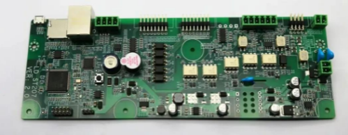
RF circuit board
5 About edging
The edge wrapping processing of the circuit board and the metallization edge wrapping processing of the surrounding network can reduce the loss of RF signals. Because the circuit board is made by splicing in the actual production process, the metallization production of the board edge requires that the shape of the metal clad edge be cut before the through hole copper sinking. At this time, the circuit board has not been finished, so the boards must be connected with each other through some connecting tapes, so they cannot be cut completely, Generally, we will place these connecting strips far away from the RF area and try to keep them as short as possible. Generally, the board factory will require two connecting strips on each side, which should not be shorter than 5mm. Generally, the microstrip line at the RF input and output place should be top to the board edge. At this position, we will require the PCB factory to have complete edge cladding. Since the edge cladding is the same network with the ground, it will be short circuited with the microstrip line, After returning to the process assembly department of our company, our circuit board is required to gently scrape an opening with a scalpel to separate it from the ground network. The reason why we do this is to make the binding as complete as possible and keep the connecting band away from the RF area
6. Treatment of RF circuit power supply
As we all know, the power supply of the circuit needs decoupling capacitors to filter the power supply to remove interference. RF chips are more sensitive to the power supply, so decoupling capacitors and isolation inductors are needed to filter the noise interference of the power supply. The power supply of the RF circuit should be filtered immediately after being introduced into the circuit board, and distributed to each part of the circuit through the voltage stabilizing block. In order to reduce current loss and generate voltage drop, The power supply should be transmitted to the required device through the blind hole in the inner layer. The power supply of RF circuit generally does not need to be divided into planes. The whole power supply plane will interfere with the RF signal. Therefore, the power supply only needs to meet the current requirements in the inner layer in the form of wire. However, in order to avoid voltage drop, the power supply wire should not be wound around as much as possible, and should be as short as possible, and should not be overlapped with the microstrip line, but also avoid loops, In addition, the power supply of the decoupling power supply around the PCB chip and the vias on the grounding pad should be placed as close as possible to the capacitive pad, and the capacitive grounding pad needs to be laid with copper sheet in a large area. Here, it should be noted that the aperture and number of vias should be selected according to the current size.


抖音二維碼

Q Q二維碼

微信二維碼
點(diǎn)擊
然后
聯(lián)系
然后
聯(lián)系
電話熱線
13410863085Q Q

微信

- 郵箱