鑫景福致力于滿足“快速服務,零缺陷,輔助研發”PCBA訂購單需求。


行業新聞
01 Type of mICro vias
PCB circuits with different characteristics on the circuit board must be separated, but they must not be connected under the best conditions that cause interference signals, so micro via must be used. Generally, the diameter of micro vias is 0.05mm~0.22mm, and these vias are generally divided into three categories, namely, blindvia, buryvia and throughvia. The buried hole is located at the top and bottom surface of the printed circuit board, and has a certain depth, which is used to connect the surface line and the lower inner line. The depth of the hole generally does not exceed a certain proportion (diameter). The buried hole refers to the connection hole located in the inner layer of the printed circuit board, which is not easy to expand to the surface layer of the pcb circuit board. The two kinds of holes are located in the inner layer of the PCB circuit board. Before laminating, the embedded hole forming PCB process is used. During the whole process of via generation, multiple inner layers will continue to be overlapped. The third type is calLED buried hole. This type of hole can be used to complete internal interconnection or as the adhesive precise positioning hole of components over all PCB.
02 Zoning method
When designing the RF circuit board, the high-power RF amplifier (HPA) and low-noise amplifier (LNA) should be protected as much as possible. In a SIMple way, the high-power RF sending circuit should be prevented from low-noise receiving circuit. If there are many indoor spaces on the PCB, this can be easily guaranteed. However, when there are many parts and components, the indoor space for PCB production and manufacturing will become SMAll, so it is impossible to do so. They can be put on both sides of the PCB board, or let them replace the work, rather than work separately. SometiMES, high-power circuits can also include RF oil buffer and voltage controlled oscillator (VCO).
The design partition can be divided into physical partition and electrical partition. The key of entity partition involves the reasonable layout, direction and shielding of components; Electrical equipment partition can be divided into power distribution, RF wiring, more sensitive circuit and data signal, grounding device and other partitions.
03 Entity partition
The reasonable Layout of components is important to complete an excellent RF design. The most effective technology is to first fix the components on the RF relative path, and adjust their direction to minimize the length of the RF relative path. RF input shall be prevented from RF output, and high-power circuits and low-noise circuits shall be prevented as far as possible.
The most effective circuit board stacking method is to distribute the main grounding device to the second layer below the surface layer, and try to walk the RF line on the surface. Minimizing the size of vias on RF relative paths can not only reduce the relative path inductance, but also reduce the empty solder joints on the main ground plane, and reduce the opportunity for RF kinetic energy leakage to other areas in the stack.
In the physical indoor space, the linear circuit like the multi-level amplifier can generally protect several RF areas from each other, but the duplexer, mixer and high-frequency amplifier have several RF/IF data signals influencing each other all the time, so be careful to minimize this hazard. RF and IF wiring shall be crossed as far as possible, and the total area of a grounding device shall be separated between them as far as possible. Proper RF relative path is critical to the characteristics of a whole PCB, which is why reasonable PCB layout of components generally takes up most of the time in mobile phone PCB design.
On the mobile phone PCB board, it is generally possible to place the low-noise amplifier circuit on one side of the PCB proofing plate, and place the high-power amplifier on the other side, which finally means that the duplexer connects them to one end of the RF wireless antenna and the other end of the baseband CPU on the same surface. There must be some methods to ensure that RF kinetic energy is not easily referred to as via, which is transmitted from one side of the board to the other. The common technical feature is to apply embedded holes on both sides. It can mean that the buried holes are distributed on both sides of the PCB board and are not affected by RF, so as to minimize the harmful effects of vias.
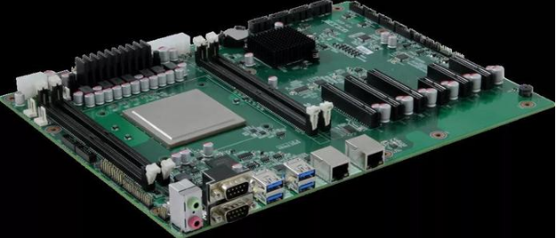
RF circuit board
04 Metal shield
Sometimes, it is unlikely to preserve sufficient differences among several circuit blockchains. In such cases, it is important to consider the use of metal shielding to shield the frequency radiation kinetic energy in the RF area. However, metal shielding also has adverse effects, such as high manufacturing costs and installation costs.
The metal shielding cover with irregular appearance design can not ensure high precision during production and manufacturing, and the square or square metal shielding cover also restricts the reasonable layout of components; Dismantlement and replacement of unfavorable parts and components of metal shielding cover and removal of common faults; Because the metal shield must be welded on the ground surface and must maintain a proper distance from the components, it must occupy precious PCB indoor space.
It is very important to ensure the details of the metal shield as much as possible. Therefore, the large digital power line entering the metal shield should go to the inner layer as much as possible, and it is better to set the next layer of the data signal route layer as a geological structure. RF power lines can be routed from the small gap at the bottom of the metal shield and the wiring layer at the opening of the grounding device. However, the periphery of the opening should be surrounded by the total area of many grounding devices as much as possible. The grounding devices on different data signal layers can mean that several vias are connected together. DeSPIte the above defects, the metal shield is still very reasonable, and is often the only solution to protect important circuits.
05 Power decoupling circuit
Proper and reasonable decoupling circuit is also crucial. Many RF integrated ics integrated with linear route are very sensitive to power supply noise. Generally, each integrated ic must select up to four capacitors and one protective inductor to filter out all power supply noise.
The minimum capacitor value generally lies in the series resonance of the capacitor itself and the inductance of the connecting pin. The value of C4 is selected from this. The values of C3 and C2 are relatively large because of the correlation of their own pin inductance, and the actual effect of RF decoupling is worse, but they are more suitable for filtering noise data signals with lower frequencies. RF decoupling is performed by the inductor L1, which makes RF data signals unable to be coupled to the IC from the power plug. Since all wiring is a potential wireless antenna that can both accept and send RF data signals, it is necessary to protect RF signals from key lines and components.
The physical part of this decoupling component is also generally important. The reasonable layout standard of these key components is: C4 should be close to the IC grounding pin and grounding device as much as possible, C3 must be close to C4, C2 must be close to C3, and the connection wiring between IC grounding pin and C4 should be as short as possible. The grounding device end (especially C4) of these components should generally mean that the first grounding structure under the surface is connected to the grounding device pin of the integrated IC. The vias connecting the components to the geological structure should be close to the component welding layer on the PCB as much as possible. It is better to use the buried holes punched on the welding layer to minimize the inductance of the electrode connecting wire, and the inductance L1 should be close to C1.


抖音二維碼

Q Q二維碼

微信二維碼
點擊
然后
聯系
然后
聯系
電話熱線
13410863085Q Q

微信

- 郵箱